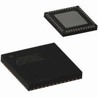
ATA5428-PLQW Atmel, ATA5428-PLQW Datasheet - Page 17

ATA5428-PLQW
Manufacturer Part Number
ATA5428-PLQW
Description
IC TXRX WIDEBND 433/868MHZ 48QFN
Manufacturer
Atmel
Specifications of ATA5428-PLQW
Frequency
433MHz, 868MHz
Data Rate - Maximum
20kbps
Modulation Or Protocol
ASK, FSK
Applications
Alarm and Security Systems, RKE
Power - Output
10dBm
Sensitivity
-112.5dBm
Voltage - Supply
2.4 V ~ 3.6 V or 4.4 V ~ 6.6 V
Current - Receiving
10.5mA
Current - Transmitting
10mA
Data Interface
PCB, Surface Mount
Antenna Connector
PCB, Surface Mount
Operating Temperature
-40°C ~ 85°C
Package / Case
48-VQFN Exposed Pad, 48-HVQFN, 48-SQFN, 48-DHVQFN
Operating Temperature (min)
-40C
Operating Temperature (max)
85C
Operating Temperature Classification
Industrial
Product Depth (mm)
7mm
Product Height (mm)
0.9mm
Product Length (mm)
7mm
Lead Free Status / RoHS Status
Lead free / RoHS Compliant
Memory Size
-
Lead Free Status / Rohs Status
Compliant
Other names
ATA5428-PLQHCT
ATA5428-PLQHCT
ATA5428-PLQWCT
ATA5428-PLQHCT
ATA5428-PLQWCT
Available stocks
Company
Part Number
Manufacturer
Quantity
Price
Company:
Part Number:
ATA5428-PLQW
Manufacturer:
LITELINK
Quantity:
106
Part Number:
ATA5428-PLQW
Manufacturer:
ATMEL/爱特梅尔
Quantity:
20 000
3.7
3.8
3.9
4841D–WIRE–10/07
In-band Disturbers, Data Filter, Quasi-peak Detector, Data Slicer
DEM_OUT Output
RSSI Output
If a disturbing signal falls into the received band or a blocker is not continuous wave, the perfor-
mance of a receiver strongly depends on the circuits after the IF filter. The demodulator, data
filter and data slicer are important, in that case.
The data filter of the ATA5423/ATA5425/ATA5428/ATA5429 implies a quasi-peak detector. This
results in a good suppression of the above mentioned disturbers and exhibits a good carrier to
Gaussian noise performance. The required useful signal to disturbing signal ratio to be received
with a BER of 10
BR_Range_2)/6 dB (BR_Range_3) in FSK mode. Due to the many different waveforms possible
these numbers are measured for signal as well as for disturbers with peak amplitude values.
Note that these values are worst case values and are valid for any type of modulation and mod-
ulating frequency of the disturbing signal as well as the receiving signal. For many combinations,
lower carrier to disturbing signal ratios are needed.
The internal raw output signal of the demodulator Demod_Out is available at pin DEM_OUT.
DEM_OUT is an open drain output and must be connected to a pull-up resistor if it is used (typi-
cally 100 k ) otherwise no signal is present at that pin.
The output voltage of the pin RSSI is an analog voltage, proportional to the input power level.
Using the RSSI output signal, the signal strength of different transmitters can be distinguished.
The usable dynamic range of the RSSI amplifier is 70 dB, the input power range P(RF
–115 dBm to –45 dBm and the gain is 8 mV/dB.
typical device at 433.92 MHz with VS1 = VS2 = 2.4 to 3.6 V and T
matched input according to
3.3 dB and at 868.3 MHz about 2.7 dB more signal level, at 345 MHz about 0.8 dB and at
315 MHz about 1 dB less signal level is needed for the same RSSI results.
Figure 3-6.
Typical RSSI Characteristic versus Temperature and Supply Voltage
–3
is less than 12 dB in ASK mode and less than 3 dB (BR_Range_0 to
1100
1000
ATA5423/ATA5425/ATA5428/ATA5429
900
800
700
600
500
400
-120
Table 3-2 on page 12
-110
min.
-100
-90
P
typ.
RF_IN
Figure 3-6
and
-80
(dBm)
Figure 3-1 on page
-70
max.
shows the RSSI characteristic of a
-60
amb
-50
= –40°C to +85°C with a
11. At 915 MHz about
-40
IN
) is
17


