ATA5428-PLQW Atmel, ATA5428-PLQW Datasheet - Page 53
ATA5428-PLQW
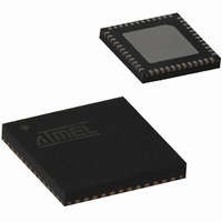
Manufacturer Part Number
ATA5428-PLQW
Description
IC TXRX WIDEBND 433/868MHZ 48QFN
Manufacturer
Atmel
Specifications of ATA5428-PLQW
Frequency
433MHz, 868MHz
Data Rate - Maximum
20kbps
Modulation Or Protocol
ASK, FSK
Applications
Alarm and Security Systems, RKE
Power - Output
10dBm
Sensitivity
-112.5dBm
Voltage - Supply
2.4 V ~ 3.6 V or 4.4 V ~ 6.6 V
Current - Receiving
10.5mA
Current - Transmitting
10mA
Data Interface
PCB, Surface Mount
Antenna Connector
PCB, Surface Mount
Operating Temperature
-40°C ~ 85°C
Package / Case
48-VQFN Exposed Pad, 48-HVQFN, 48-SQFN, 48-DHVQFN
Operating Temperature (min)
-40C
Operating Temperature (max)
85C
Operating Temperature Classification
Industrial
Product Depth (mm)
7mm
Product Height (mm)
0.9mm
Product Length (mm)
7mm
Lead Free Status / RoHS Status
Lead free / RoHS Compliant
Memory Size
-
Lead Free Status / Rohs Status
Compliant
Other names
ATA5428-PLQHCT
ATA5428-PLQHCT
ATA5428-PLQWCT
ATA5428-PLQHCT
ATA5428-PLQWCT
Available stocks
Company
Part Number
Manufacturer
Quantity
Price
Company:

Part Number:
ATA5428-PLQW
Manufacturer:
LITELINK
Quantity:
106
Part Number:
ATA5428-PLQW
Manufacturer:
ATMEL/爱特梅尔
Quantity:
20 000


9.1.2
9.1.3
4841D–WIRE–10/07
Sleep Mode
Start-up Mode
To save current it is recommended that CLK and V
does not include the current of the Microcontroller_Interface, I
device connected to pin VSOUT (for example, microcontroller). If CLK and/or VSOUT is enabled
during RX polling mode the current consumption is calculated as follows:
During T
nal. To guarantee the reception of a transmitted command, the transmitter must start the
telegram with an adequate preburst. The required length of the preburst, T
the polling parameters T
the actual bit rate and the number of bits (N
The length of period T
factor X
calculated to be:
In US and European applications, the maximum value of T
(which is done by setting the bit X
1.2 ms in that case. The sleep time can be extended to about 300 ms by setting X
(which is done by setting X
9.6 ms.
During T
circuit starts up (T
ready to receive.
I
T
T
S_Poll
Preburst
Sleep
=
=
Sleep
I
Sleep
Sleep
Startup_PLL
P
T
+
Sleep
I
, T
defined by the bit X
VSINT
+
Startup_PLL
1024
T
+
Startup_PLL
the PLL is enabled and starts up. If the PLL is locked, the signal processing
Startup_Sig_Proc
I
EXT
Sleep
ATA5423/ATA5425/ATA5428/ATA5429
T
Sleep
DCLK
and T
is defined by the 5-bit word sleep in control register 4, the extension
+
, T
Sleep
T
Startup_Sig_Proc
Startup_Sig_Proc
Startup_PLL
X
). After the start-up time all circuits are in stable condition and
Sleep
Sleep
in control register 4 to “1”), the time resolution is then about
Sleep
in control register 4, and the basic clock cycle T
in control register 4 to “0”). The time resolution is about
, T
Startup_Sig_Proc
, the transceiver is not sensitive to a transmitter sig-
+
Bit-check
T
Bit_check
VSOUT
) to be tested.
and T
be disabled during RX polling mode. I
Sleep
Bit-check
VSINT
is about 38 ms if X
, or the current of an external
. Thus, T
Preburst
Bit-check
Sleep
, depends on
depends on
is set to 1
DCLK
Sleep
. It is
to 8
53
P
Related parts for ATA5428-PLQW
Image
Part Number
Description
Manufacturer
Datasheet
Request
R

Part Number:
Description:
RF Transceiver ASK/FSK Transceiver 434 and 868MHz
Manufacturer:
Atmel
Datasheet:
Part Number:
Description:
RF Transceiver ASK/FSK Transceiver 434 and 868MHz
Manufacturer:
Atmel
Datasheet:
Part Number:
Description:
RF Transceiver ASK/FSK Transceiver 434 and 868 MHz
Manufacturer:
Atmel
Datasheet:

Part Number:
Description:
Manufacturer:
Atmel
Datasheet:
Part Number:
Description:
Manufacturer:
Atmel
Datasheet:

Part Number:
Description:
Uhf Ask/fsk Transceiver
Manufacturer:
ATMEL Corporation
Datasheet:

Part Number:
Description:
DEV KIT FOR AVR/AVR32
Manufacturer:
Atmel
Datasheet:
Part Number:
Description:
INTERVAL AND WIPE/WASH WIPER CONTROL IC WITH DELAY
Manufacturer:
ATMEL Corporation
Datasheet:
Part Number:
Description:
Low-Voltage Voice-Switched IC for Hands-Free Operation
Manufacturer:
ATMEL Corporation
Datasheet:
Part Number:
Description:
MONOLITHIC INTEGRATED FEATUREPHONE CIRCUIT
Manufacturer:
ATMEL Corporation
Datasheet:
Part Number:
Description:
AM-FM Receiver IC U4255BM-M
Manufacturer:
ATMEL Corporation
Datasheet:
Part Number:
Description:
Monolithic Integrated Feature Phone Circuit
Manufacturer:
ATMEL Corporation
Datasheet: