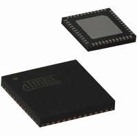
ATA5428-PLQW Atmel, ATA5428-PLQW Datasheet - Page 78

ATA5428-PLQW
Manufacturer Part Number
ATA5428-PLQW
Description
IC TXRX WIDEBND 433/868MHZ 48QFN
Manufacturer
Atmel
Specifications of ATA5428-PLQW
Frequency
433MHz, 868MHz
Data Rate - Maximum
20kbps
Modulation Or Protocol
ASK, FSK
Applications
Alarm and Security Systems, RKE
Power - Output
10dBm
Sensitivity
-112.5dBm
Voltage - Supply
2.4 V ~ 3.6 V or 4.4 V ~ 6.6 V
Current - Receiving
10.5mA
Current - Transmitting
10mA
Data Interface
PCB, Surface Mount
Antenna Connector
PCB, Surface Mount
Operating Temperature
-40°C ~ 85°C
Package / Case
48-VQFN Exposed Pad, 48-HVQFN, 48-SQFN, 48-DHVQFN
Operating Temperature (min)
-40C
Operating Temperature (max)
85C
Operating Temperature Classification
Industrial
Product Depth (mm)
7mm
Product Height (mm)
0.9mm
Product Length (mm)
7mm
Lead Free Status / RoHS Status
Lead free / RoHS Compliant
Memory Size
-
Lead Free Status / Rohs Status
Compliant
Other names
ATA5428-PLQHCT
ATA5428-PLQHCT
ATA5428-PLQWCT
ATA5428-PLQHCT
ATA5428-PLQWCT
Available stocks
Company
Part Number
Manufacturer
Quantity
Price
Company:
Part Number:
ATA5428-PLQW
Manufacturer:
LITELINK
Quantity:
106
Part Number:
ATA5428-PLQW
Manufacturer:
ATMEL/爱特梅尔
Quantity:
20 000
12. Electrical Characteristics: General (Continued)
This device is manufactured with an industrial (not automotive) grade process and process controls. Although this device may
meet certain automotive grade criteria in performance, Atmel can not recommend that this device be used in any automotive
application.
All parameters refer to GND and are valid for T
and V
about current consumption, timing and digital pin properties can be found in the specific sections of the “Electrical Characteristics”.
78
*) Type means: A = 100% tested, B = 100% correlation tested, C = Characterized on samples, D = Design parameter
Note:
4.10
No. Parameters
4.6
4.7
4.8
4.9
VS2
Pulling of radio frequency
f
C
and supply changes
Amplitude XTAL after
start
Real part of XTO
impedance at start
Maximum series
resistance R
after start
Nominal XTAL load
resonant frequency
RF
L2
= V
1. Pin numbers in brackets mean they were measured with RF_IN matched to 50 according to
due to XTO, C
ATA5423/ATA5425/ATA5428/ATA5429
versus temperature
-
up
VAUX
component values according to
with component values according to
-
= 5.0V (Base
up
m
of XTAL
L1
-
up
and
-
station Application). Typical values are given at f
Test Conditions
1.0 pF
C
R
PLL adjusted with
FREQ at nominal
temperature and supply
voltage
C
R
V(XTAL1, XTAL2)
peak
V(XTAL1)
peak
C
start impedance, this
value is important for
crystal oscillator startup
C
C
f
f
f
f
f
RF
RF
RF
RF
RF
m
m
m
m
0
0
m
= 315 MHz
= 345 MHz
= 433.92 MHz
= 868.3 MHz
= 915 MHz
= 5 fF, C
120
2.2 pF, small signal
15
2.2 pF
-
-
14 fF
14.0 fF
to
to
-
-
peak value
peak value
C
0
Table 3-2 on page 12
0
amb
= 1.8 pF
2.2 pF
Table 3-7 on page
= 25°C, V
VS1
24, 25
24, 25
24, 25
24, 25
24, 25
Pin
4, 10
= V
(1)
VS2
and RF_OUT matched to 50 according to
22.
= 3.0V (1
Symbol
V
V
R
Re
PPXTAL
PPXTAL
f
m_max
f
XTAL
XTO2
XTO
-
RF
battery application), V
= 433.92 MHz unless otherwise specified. Details
Min.
–
2
12.73193
13.94447
13.25311
13.41191
14.13324
–
Typ.
2,000
700
350
15
VS2
= 6.0V (2-battery application)
Figure 3-1 on page 11
–
Figure 3-10 on page 21
Max.
1,500
120
+2
4841D–WIRE–10/07
mVpp
mVpp
Unit
ppm
MHz
MHz
MHz
MHz
MHz
Type*
with
C
C
C
B
B
D


