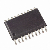
ATA3745P3-TGQY Atmel, ATA3745P3-TGQY Datasheet - Page 4

ATA3745P3-TGQY
Manufacturer Part Number
ATA3745P3-TGQY
Description
IC UHF ASK/FSK RECEIVER 20SOIC
Manufacturer
Atmel
Datasheet
1.ATA3745P3-TGSY.pdf
(30 pages)
Specifications of ATA3745P3-TGQY
Frequency
310MHz ~ 440MHz
Sensitivity
-108dBm
Data Rate - Maximum
10 kBaud
Modulation Or Protocol
ASK, FSK
Applications
RKE, TPM, Security Systems
Current - Receiving
7mA
Data Interface
PCB, Surface Mount
Antenna Connector
PCB, Surface Mount
Voltage - Supply
4.5 V ~ 5.5 V
Operating Temperature
-40°C ~ 85°C
Package / Case
20-SOIC (0.300", 7.50mm Width)
Operating Temperature (min)
-40C
Operating Temperature (max)
85C
Operating Temperature Classification
Industrial
Operating Supply Voltage (min)
4.5V
Operating Supply Voltage (typ)
5V
Operating Supply Voltage (max)
5.5V
Lead Free Status / RoHS Status
Lead free / RoHS Compliant
Features
-
Memory Size
-
Lead Free Status / Rohs Status
Compliant
Other names
ATA3745P3-TGQYTR
Available stocks
Company
Part Number
Manufacturer
Quantity
Price
Company:
Part Number:
ATA3745P3-TGQY
Manufacturer:
Atmel
Quantity:
1 973
3. RF Front End
4
ATA3745
The RF front end of the receiver is a heterodyne configuration that converts the input signal
into a 1-MHz IF signal. As shown in the block diagram, the front end consists of an LNA (low
noise amplifier), LO (local oscillator), a mixer and an RF amplifier.
The LO generates the carrier frequency for the mixer via a PLL synthesizer. The XTO (crystal
oscillator) generates the reference frequency f
generates the drive voltage frequency f
LF. f
quency detector. The current output of the phase frequency detector is connected to a passive
loop filter and thereby generates the control voltage V
uration, V
calculated using the following formula:
The XTO is a one-pin oscillator that operates at the series resonance of the quartz crystal.
ure
value of that capacitor is recommended by the crystal supplier. The value of CL should be opti-
mized for the individual board layout to achieve the exact value of f
When designing the system in terms of receiving bandwidth, the accuracy of the crystal and
XTO must be considered.
Figure 3-1.
The passive loop filter connected to pin LF is designed for a loop bandwidth of
B
Figure 3-1
width. If the filter components are changed for any reason, please note that the maximum
capacitive load at pin LF is limited. If the capacitive load is exceeded, a bit check may no
longer be possible since f
incoming data stream. Therefore, self polling also does not work in that case.
f
mula:
f
LO
XTO
Loop
is determined by the RF input frequency f
3-1shows the proper layout, with the crystal connected to GND via a capacitor CL. The
LO
=
= 100 kHz. This value for B
f
LO
is divided by a factor of 64. The divided frequency is compared to f
f
------- -
64
LO
LF
=
shows the appropriate loop filter components to achieve the desired loop band-
f
is controlled such that f
RF
PLL Peripherals
–
f
IF
LO
cannot settle in time before the bit check starts to evaluate the
Loop
LFGND
LFVCC
DVCC
XTO
LO
exhibits the best possible noise performance of the LO.
LF
LO
/ 64 is equal to f
for the mixer. f
V
V
S
S
RF
and the IF frequency f
XTO
4.7 nF
. The VCO (voltage-controlled oscillator)
R
820
C
1
9
LF
C
for the VCO. By means of that config-
XTO
LO
L
is dependent on the voltage at pin
1 nF
. If f
C
10
LO
is determined, f
IF
XTO
using the following for-
XTO
and thereby of f
by the phase fre-
4901B–RKE–11/07
XTO
can be
Fig-
LO
.


