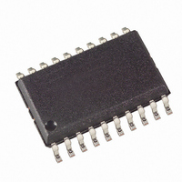
ATA3745P3-TGQY Atmel, ATA3745P3-TGQY Datasheet - Page 12

ATA3745P3-TGQY
Manufacturer Part Number
ATA3745P3-TGQY
Description
IC UHF ASK/FSK RECEIVER 20SOIC
Manufacturer
Atmel
Datasheet
1.ATA3745P3-TGSY.pdf
(30 pages)
Specifications of ATA3745P3-TGQY
Frequency
310MHz ~ 440MHz
Sensitivity
-108dBm
Data Rate - Maximum
10 kBaud
Modulation Or Protocol
ASK, FSK
Applications
RKE, TPM, Security Systems
Current - Receiving
7mA
Data Interface
PCB, Surface Mount
Antenna Connector
PCB, Surface Mount
Voltage - Supply
4.5 V ~ 5.5 V
Operating Temperature
-40°C ~ 85°C
Package / Case
20-SOIC (0.300", 7.50mm Width)
Operating Temperature (min)
-40C
Operating Temperature (max)
85C
Operating Temperature Classification
Industrial
Operating Supply Voltage (min)
4.5V
Operating Supply Voltage (typ)
5V
Operating Supply Voltage (max)
5.5V
Lead Free Status / RoHS Status
Lead free / RoHS Compliant
Features
-
Memory Size
-
Lead Free Status / Rohs Status
Compliant
Other names
ATA3745P3-TGQYTR
Available stocks
Company
Part Number
Manufacturer
Quantity
Price
Company:
Part Number:
ATA3745P3-TGQY
Manufacturer:
Atmel
Quantity:
1 973
Figure 5-2.
Figure 5-3.
12
ATA3745
Polling Mode Flow Chart
Timing Diagram for a Completely Successful Bit Check
(Number of checked Bits: 3)
Enable IC
Bit check
Dem_out
Data
NO
Sleep Mode:
All circuits for signal processing are
disabled. Only XTO and Polling logic are
enabled.
I
T
Start-up Mode:
The signal processing circuits are
enabled. After the start-up time (T
all circuits are in stable
condition and ready to receive.
I
T
Bit-check Mode:
The incoming data stream is
analyzed. If the timing indicates a valid
transmitter signal, the receiver is set to
receiving mode. Otherwise it is set to
Sleep mode.
I
T
Receiving Mode:
The receiver is turned on permanently
and passes the data stream to the
connected microcontroller.
It can be set to Sleep mode through an
OFF command via pin DATA or ENABLE
I
S
S
S
S
Sleep
Startup
Bit-check
= I
= I
= I
= I
SON
SON
SON
SON
Polling mode
= Sleep
OFF Command
Bit Check
X
OK ?
Sleep
YES
1024
1/2 Bit
T
Startup
Clk
1/2 Bit
)
1/2 Bit
Bit check ok
1/2 Bit
Sleep:
X
T
T
X
Clk
Startup
Sleep
Bit-check
:
:
1/2 Bit
:
:
5-bit word defined by Sleep0 to
Sleep4 in OPMODE register
Extension factor defined by
X
Basic clock cycle defined by f
and pin MODE
Is defined by the selected baud-rate
range and T
is defined by Baud0 and Baud1 in
the OPMODE register.
Depends on the result of the bit check.
If the bit check is ok, T
depends on the number of bits to be
checked (N
utilized data rate.
If the bit check fails, the average
time period for that check depends
on the selected baud-rate range and
on T
defined by Baud0 and Baud1 in the
OPMODE register.
SleepTemp
1/2 Bit
Clk
. The baud-rate range is
according to Table 5-7
Bit-check
Clk
. The baud-rate range
Receiving mode
) and on the
Bit-check
XTO
4901B–RKE–11/07


