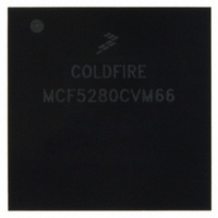
MCF5280CVM66 Freescale Semiconductor, MCF5280CVM66 Datasheet - Page 261

MCF5280CVM66
Manufacturer Part Number
MCF5280CVM66
Description
IC MPU 32BIT COLDF 256-MAPBGA
Manufacturer
Freescale Semiconductor
Series
MCF528xr
Datasheet
1.MCF5216CVM66J.pdf
(766 pages)
Specifications of MCF5280CVM66
Core Processor
Coldfire V2
Core Size
32-Bit
Speed
66MHz
Connectivity
CAN, EBI/EMI, Ethernet, I²C, SPI, UART/USART
Peripherals
DMA, LVD, POR, PWM, WDT
Number Of I /o
142
Program Memory Type
ROMless
Ram Size
64K x 8
Voltage - Supply (vcc/vdd)
2.7 V ~ 3.6 V
Data Converters
A/D 8x10b
Oscillator Type
External
Operating Temperature
-40°C ~ 85°C
Package / Case
256-MAPBGA
Controller Family/series
ColdFire
No. Of I/o's
150
Program Memory Size
2KB
Ram Memory Size
64KB
Cpu Speed
66.67MHz
Embedded Interface Type
CAN, I2C, SPI, UART
No. Of Pwm Channels
8
Rohs Compliant
Yes
Lead Free Status / RoHS Status
Lead free / RoHS Compliant
Eeprom Size
-
Program Memory Size
-
Available stocks
Company
Part Number
Manufacturer
Quantity
Price
Company:
Part Number:
MCF5280CVM66
Manufacturer:
FREESCAL
Quantity:
151
Company:
Part Number:
MCF5280CVM66
Manufacturer:
Freescale Semiconductor
Quantity:
10 000
Company:
Part Number:
MCF5280CVM66J
Manufacturer:
Freescale Semiconductor
Quantity:
10 000
Company:
Part Number:
MCF5280CVM66L
Manufacturer:
FREESCAL
Quantity:
151
- Current page: 261 of 766
- Download datasheet (9Mb)
Signal Descriptions
14.2.1.10 Transfer In Progress (TIP)
The TIP output is asserted indicating a bus transfer is in progress. It is negated during idle bus cycles. Note
that TIP is held asserted on back-to-back cycles.
NOTE
TIP is not asserted during SDRAM accesses.
This pin can also be configured as GPIO PE0 or SYNCB.
14.2.1.11 Chip Selects (CS[6:0])
Each chip select can be programmed for a base address location and for masking addresses, port size and
burst-capability indication, wait-state generation, and internal/external termination.
Reset clears all chip select programming; CS0 is the only chip select initialized out of reset. CS0 is also
unique because it can function at reset as a global chip select that allows boot ROM to be selected at any
defined address space. The port size for boot CS0 is set during chip configuration by the levels on D[19:18]
on the rising edge of RSTI, as described in
Chapter 27, “Chip Configuration Module
(CCM).” The
chip-select implementation is described in
Chapter 12, “Chip Select
Module.”
These pins can also be configured as A[23:21] and GPIO PJ[3:0].
14.2.2
SDRAM Controller Signals
These signals are used for SDRAM accesses.
14.2.2.1 SDRAM Row Address Strobe (SRAS)
This output is the SDRAM synchronous row address strobe.
This pin is configured as GPIO PSD5 in single-chip mode.
14.2.2.2 SDRAM Column Address Strobe (SCAS)
This output is the SDRAM synchronous column address strobe.
This pin is configured as GPIO PSD4 in single-chip mode.
14.2.2.3 SDRAM Write Enable (DRAMW)
The DRAM write signal (DRAMW) is asserted to signify that a DRAM write cycle is underway. A read
cycle is indicated by the negation of DRAMW.
This pin is configured as GPIO PSD3 in single-chip mode.
14.2.2.4 SDRAM Bank Selects (SDRAM_CS[1:0])
These signals interface to the chip-select lines of the SDRAMs within a memory block. Thus, there is one
SDRAM_CS line for each memory block (the processor supports two SDRAM memory blocks).
These pins is configured as GPIO PSD[2:1] in single-chip mode.
MCF5282 and MCF5216 ColdFire Microcontroller User’s Manual, Rev. 3
Freescale Semiconductor
14-21
Related parts for MCF5280CVM66
Image
Part Number
Description
Manufacturer
Datasheet
Request
R
Part Number:
Description:
Manufacturer:
Freescale Semiconductor, Inc
Datasheet:
Part Number:
Description:
Manufacturer:
Freescale Semiconductor, Inc
Datasheet:
Part Number:
Description:
Manufacturer:
Freescale Semiconductor, Inc
Datasheet:
Part Number:
Description:
Manufacturer:
Freescale Semiconductor, Inc
Datasheet:
Part Number:
Description:
Manufacturer:
Freescale Semiconductor, Inc
Datasheet:
Part Number:
Description:
Manufacturer:
Freescale Semiconductor, Inc
Datasheet:
Part Number:
Description:
Manufacturer:
Freescale Semiconductor, Inc
Datasheet:
Part Number:
Description:
Manufacturer:
Freescale Semiconductor, Inc
Datasheet:
Part Number:
Description:
Manufacturer:
Freescale Semiconductor, Inc
Datasheet:
Part Number:
Description:
Manufacturer:
Freescale Semiconductor, Inc
Datasheet:
Part Number:
Description:
Manufacturer:
Freescale Semiconductor, Inc
Datasheet:
Part Number:
Description:
Manufacturer:
Freescale Semiconductor, Inc
Datasheet:
Part Number:
Description:
Manufacturer:
Freescale Semiconductor, Inc
Datasheet:
Part Number:
Description:
Manufacturer:
Freescale Semiconductor, Inc
Datasheet:
Part Number:
Description:
Manufacturer:
Freescale Semiconductor, Inc
Datasheet:


