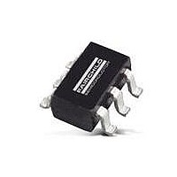
FDC3535 Fairchild Semiconductor, FDC3535 Datasheet - Page 3

FDC3535
Manufacturer Part Number
FDC3535
Description
MOSFET P-CH 80V 6-SSOT
Manufacturer
Fairchild Semiconductor
Series
PowerTrench®r
Datasheet
1.FDC3535.pdf
(7 pages)
Specifications of FDC3535
Fet Type
MOSFET P-Channel, Metal Oxide
Fet Feature
Logic Level Gate
Rds On (max) @ Id, Vgs
183 mOhm @ 2.1A, 10V
Drain To Source Voltage (vdss)
80V
Current - Continuous Drain (id) @ 25° C
2.1A
Vgs(th) (max) @ Id
3V @ 250µA
Gate Charge (qg) @ Vgs
20nC @ 10V
Input Capacitance (ciss) @ Vds
880pF @ 40V
Power - Max
700mW
Mounting Type
Surface Mount
Package / Case
*
Transistor Polarity
P-Channel
Resistance Drain-source Rds (on)
147 mOhms
Gate Charge Qg
14 nC
Forward Transconductance Gfs (max / Min)
6.3 S
Drain-source Breakdown Voltage
- 80 V
Gate-source Breakdown Voltage
20 V
Continuous Drain Current
- 2.1 A
Power Dissipation
1.6 W
Maximum Operating Temperature
+ 150 C
Mounting Style
SMD/SMT
Minimum Operating Temperature
- 55 C
Lead Free Status / RoHS Status
Lead free / RoHS Compliant
Other names
FDC3535TR
Available stocks
Company
Part Number
Manufacturer
Quantity
Price
Part Number:
FDC3535
Manufacturer:
FAIRCHILD/仙童
Quantity:
20 000
Part Number:
FDC3535-NL
Manufacturer:
FAIRCHILD/仙童
Quantity:
20 000
©2010 Fairchild Semiconductor Corporation
FDC3535 Rev. C
Typical Characteristics
10
8
6
4
2
0
2.0
1.8
1.6
1.4
1.2
1.0
0.8
0.6
0.4
10
Figure 3. Normalized On- Resistance
0
8
6
4
2
0
Figure 1.
-75
1
Figure 5. Transfer Characteristics
V
PULSE DURATION = 80
DUTY CYCLE = 0.5% MAX
V
GS
DS
I
V
D
-V
-50
GS
= -5 V
= -10 V
vs Junction Temperature
= - 2.1 A
DS
= -10 V
1
, DRAIN TO SOURCE VOLTAGE (V)
-V
T
T
J
-25
GS
On-Region Characteristics
J
= 150
,
2
PULSE DURATION = 80
DUTY CYCLE = 0.5% MAX
JUNCTION TEMPERATURE (
, GATE TO SOURCE VOLTAGE (V)
o
0
C
2
V
GS
25
T
μ
J
s
= -4.5 V
= -55
3
T
J
= 25
50
T
3
J
o
C
= 25 °C unless otherwise noted
o
C
μ
75
s
V
V
4
V
o
4
GS
100 125 150
GS
GS
C )
= -3.5 V
= -2.5 V
= -3 V
5
5
3
0.001
0.01
600
500
400
300
200
100
0.1
20
10
4
3
2
1
0
1
0.0
Figure 2.
Figure 4.
0
2
Forward Voltage vs Source Current
vs Drain Current and Gate Voltage
Figure 6.
PULSE DURATION = 80
DUTY CYCLE = 0.5% MAX
V
GS
-V
V
GS
0.2
SD
= 0 V
-V
T
, BODY DIODE FORWARD VOLTAGE (V)
= -2.5 V
GS
J
2
Normalized On-Resistance
= 150
-
, GATE TO SOURCE VOLTAGE (V)
On-Resistance vs Gate to
I
4
D
Source Voltage
,
Source to Drain Diode
I
T
D
DRAIN CURRENT (A)
J
T
0.4
= -2.1 A
o
J
= 125
C
= 25
4
o
o
C
μ
C
V
s
0.6
GS
6
PULSE DURATION = 80
DUTY CYCLE = 0.5% MAX
= -3 V
V
GS
6
= -4.5 V
V
GS
0.8
T
= -3.5 V
J
= -55
T
8
J
= 25
V
8
www.fairchildsemi.com
GS
o
1.0
C
= -10 V
o
C
μ
s
1.2
10
10


