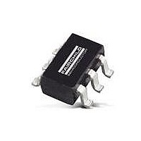
FDC3535 Fairchild Semiconductor, FDC3535 Datasheet
Home Discrete Semiconductor Products MOSFETs, GaNFETs - Single FDC3535
Manufacturer Part Number
FDC3535
Description
MOSFET P-CH 80V 6-SSOT
Manufacturer
Fairchild Semiconductor
Specifications of FDC3535
Fet Type
MOSFET P-Channel, Metal Oxide
Fet Feature
Logic Level Gate
Rds On (max) @ Id, Vgs
183 mOhm @ 2.1A, 10V
Drain To Source Voltage (vdss)
80V
Current - Continuous Drain (id) @ 25° C
2.1A
Vgs(th) (max) @ Id
3V @ 250µA
Gate Charge (qg) @ Vgs
20nC @ 10V
Input Capacitance (ciss) @ Vds
880pF @ 40V
Power - Max
700mW
Mounting Type
Surface Mount
Package / Case
*
Transistor Polarity
P-Channel
Resistance Drain-source Rds (on)
147 mOhms
Gate Charge Qg
14 nC
Forward Transconductance Gfs (max / Min)
6.3 S
Drain-source Breakdown Voltage
- 80 V
Gate-source Breakdown Voltage
20 V
Continuous Drain Current
- 2.1 A
Power Dissipation
1.6 W
Maximum Operating Temperature
+ 150 C
Mounting Style
SMD/SMT
Minimum Operating Temperature
- 55 C
Lead Free Status / RoHS Status
Lead free / RoHS Compliant
Other names
FDC3535TR
Available stocks
Manufacturer:
FAIRCHILD/仙童
Manufacturer:
FAIRCHILD/仙童
©2010 Fairchild Semiconductor Corporation
FDC3535 Rev. C
MOSFET Maximum Ratings
Thermal Characteristics
Package Marking and Ordering Information
FDC3535
P-Channel Power Trench
-80 V, -2.1 A, 183 mΩ
Features
V
V
I
E
P
T
R
R
D
DS
GS
AS
D
J
θJC
θJA
, T
Max r
Max r
High performance trench technology for extremely low r
High power and current handling capability in a widely used
surface mount package
Fast switching speed
100% UIL Tested
RoHS Compliant
Symbol
Device Marking
STG
DS(on)
DS(on)
.535
= 183 mΩ at V
= 233 mΩ at V
Drain to Source Voltage
Gate to Source Voltage
Drain Current -Continuous
Single Pulse Avalanche Energy
Power Dissipation
Power Dissipation
Operating and Storage Junction Temperature Range
Thermal Resistance, Junction to Case
Thermal Resistance, Junction to Ambient
D
D
Pin 1
SuperSOT
GS
GS
S
-Pulsed
= -10 V, I
= -4.5 V, I
FDC3535
Device
TM
D
D
-6
D
= -2.1 A
= -1.9 A
T
D
A
®
= 25 °C unless otherwise noted
G
Parameter
MOSFET
DS(on)
Package
SSOT-6
1
General Description
This
Semiconductor‘s advanced Power Trench
been optimized for r
ruggedness.
Applications
Load Switch
Synchronous Rectifier
P-Channel
Reel Size
S
D
D
7 ’’
(Note 1a)
(Note 1a)
(Note 1b)
(Note 1a)
4
5
6
(Note 3)
MOSFET
DS(on)
Tape Width
, switching performance and
is
8 mm
-55 to +150
Ratings
produced using Fairchild
-2.1
±20
-80
-10
1.6
0.7
30
78
37
®
3
2
1
process that has
June 2010
www.fairchildsemi.com
3000 units
Quantity
G
D
D
Units
°C/W
mJ
°C
W
V
V
A
Related parts for FDC3535
FDC3535 Summary of contents
... Thermal Resistance, Junction to Case θJC R Thermal Resistance, Junction to Ambient θJA Package Marking and Ordering Information Device Marking Device .535 FDC3535 ©2010 Fairchild Semiconductor Corporation FDC3535 Rev. C ® MOSFET General Description = -2.1 A This P-Channel D Semiconductor‘s advanced Power Trench = -1 been optimized for r ruggedness ...
... R is guaranteed by design while R is determined by the user's board design. θJC θCA 2. Pulse Test: Pulse Width < 300 μs, Duty cycle < 2 Starting mH ©2010 Fairchild Semiconductor Corporation FDC3535 Rev °C unless otherwise noted J Test Conditions = -250 μ -250 μA, referenced to 25 ° - ...
... Figure 3. Normalized On- Resistance vs Junction Temperature 10 μ PULSE DURATION = 80 s DUTY CYCLE = 0.5% MAX 150 - GATE TO SOURCE VOLTAGE (V) GS Figure 5. Transfer Characteristics ©2010 Fairchild Semiconductor Corporation FDC3535 Rev °C unless otherwise noted -3 μ -2 600 500 400 300 200 100 50 75 100 125 150 ...
... THIS AREA IS LIMITED BY r DS(on) 0.1 SINGLE PULSE MAX RATED o C 175 θ 0.01 0.005 0 DRAIN to SOURCE VOLTAGE (V) DS Figure 11. Forward Bias Safe Operating Area ©2010 Fairchild Semiconductor Corporation FDC3535 Rev °C unless otherwise noted J 1000 100 2 100 ...
... Typical Characteristics 2 DUTY CYCLE-DESCENDING ORDER 0.5 0.2 0.1 0.05 0.1 0.02 0.01 0.01 0.001 - Figure 13. Junction-to-Ambient Transient Thermal Response Curve ©2010 Fairchild Semiconductor Corporation FDC3535 Rev °C unless otherwise noted J SINGLE PULSE 175 C/W θ RECTANGULAR PULSE DURATION (sec NOTES: DUTY FACTOR ...
... Dimensional Outline and Pad Layout ©2010 Fairchild Semiconductor Corporation FDC3535 Rev www.fairchildsemi.com ...
... Product Status Advance Information Formative / In Design Preliminary First Production No Identification Needed Full Production Obsolete Not In Production ©2010 Fairchild Semiconductor Corporation FDC3535 Rev. C F-PFS™ Power-SPM™ ® FRFET PowerTrench SM Global Power Resource PowerXS™ Green FPS™ Programmable Active Droop™ ...
Related keywords
FDC3535 datasheet FDC3535 data sheet FDC3535 pdf datasheet FDC3535 component FDC3535 part FDC3535 distributor FDC3535 RoHS FDC3535 datasheet download


