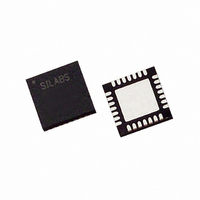
C8051F321R Silicon Laboratories Inc, C8051F321R Datasheet - Page 47

C8051F321R
Manufacturer Part Number
C8051F321R
Description
IC 8051 MCU 16K FLASH 28MLP
Manufacturer
Silicon Laboratories Inc
Series
C8051F32xr
Datasheet
1.C8051F320R.pdf
(256 pages)
Specifications of C8051F321R
Core Processor
8051
Core Size
8-Bit
Speed
25MHz
Connectivity
SMBus (2-Wire/I²C), SPI, UART/USART, USB
Peripherals
Brown-out Detect/Reset, POR, PWM, Temp Sensor, WDT
Number Of I /o
21
Program Memory Size
16KB (16K x 8)
Program Memory Type
FLASH
Ram Size
2.25K x 8
Voltage - Supply (vcc/vdd)
2.7 V ~ 3.6 V
Data Converters
A/D 13x10b
Oscillator Type
Internal
Operating Temperature
-40°C ~ 85°C
Package / Case
28-VQFN Exposed Pad, 28-HVQFN, 28-SQFN, 28-DHVQFN
Lead Free Status / RoHS Status
Contains lead / RoHS non-compliant
Eeprom Size
-
Other names
336-1067-2
- Current page: 47 of 256
- Download datasheet (4Mb)
Bits7-3:
Bit2:
Bits1-0:
Bits7-0:
AD0SC4
R/W
R/W
Bit7
Bit7
AD0SC4-0: ADC0 SAR Conversion Clock Period Bits.
SAR Conversion clock is derived from system clock by the following equation, where AD0SC refers
to the 5-bit value held in bits AD0SC4-0. SAR Conversion clock requirements are given in Table 5.1.
AD0LJST: ADC0 Left Justify Select.
0: Data in ADC0H:ADC0L registers are right-justified.
1: Data in ADC0H:ADC0L registers are left-justified.
UNUSED. Read = 00b; Write = don’t care.
ADC0 Data Word High-Order Bits.
For AD0LJST = 0: Bits 7-2 are the sign extension of Bit1. Bits 1-0 are the upper 2 bits of the 10-bit
ADC0 Data Word.
For AD0LJST = 1: Bits 7-0 are the most-significant bits of the 10-bit ADC0 Data Word.
AD0SC
AD0SC3
R/W
R/W
Bit6
Bit6
=
Figure 5.8. ADC0H: ADC0 Data Word MSB Register
Figure 5.7. ADC0CF: ADC0 Configuration Register
SYSCLK
--------------------- - 1
CLK
AD0SC2
R/W
R/W
Bit5
Bit5
SAR
–
AD0SC1
R/W
R/W
Bit4
Bit4
AD0SC0
R/W
R/W
Bit3
Bit3
Rev. 1.1
AD0LJST
R/W
R/W
Bit2
Bit2
R/W
R/W
Bit1
Bit1
-
C8051F320/1
R/W
R/W
Bit0
Bit0
-
SFR Address:
SFR Address:
00000000
Reset Value
11111000
Reset Value
0xBC
0xBE
47
Related parts for C8051F321R
Image
Part Number
Description
Manufacturer
Datasheet
Request
R
Part Number:
Description:
SMD/C°/SINGLE-ENDED OUTPUT SILICON OSCILLATOR
Manufacturer:
Silicon Laboratories Inc
Part Number:
Description:
Manufacturer:
Silicon Laboratories Inc
Datasheet:
Part Number:
Description:
N/A N/A/SI4010 AES KEYFOB DEMO WITH LCD RX
Manufacturer:
Silicon Laboratories Inc
Datasheet:
Part Number:
Description:
N/A N/A/SI4010 SIMPLIFIED KEY FOB DEMO WITH LED RX
Manufacturer:
Silicon Laboratories Inc
Datasheet:
Part Number:
Description:
N/A/-40 TO 85 OC/EZLINK MODULE; F930/4432 HIGH BAND (REV E/B1)
Manufacturer:
Silicon Laboratories Inc
Part Number:
Description:
EZLink Module; F930/4432 Low Band (rev e/B1)
Manufacturer:
Silicon Laboratories Inc
Part Number:
Description:
I°/4460 10 DBM RADIO TEST CARD 434 MHZ
Manufacturer:
Silicon Laboratories Inc
Part Number:
Description:
I°/4461 14 DBM RADIO TEST CARD 868 MHZ
Manufacturer:
Silicon Laboratories Inc
Part Number:
Description:
I°/4463 20 DBM RFSWITCH RADIO TEST CARD 460 MHZ
Manufacturer:
Silicon Laboratories Inc
Part Number:
Description:
I°/4463 20 DBM RADIO TEST CARD 868 MHZ
Manufacturer:
Silicon Laboratories Inc
Part Number:
Description:
I°/4463 27 DBM RADIO TEST CARD 868 MHZ
Manufacturer:
Silicon Laboratories Inc
Part Number:
Description:
I°/4463 SKYWORKS 30 DBM RADIO TEST CARD 915 MHZ
Manufacturer:
Silicon Laboratories Inc
Part Number:
Description:
N/A N/A/-40 TO 85 OC/4463 RFMD 30 DBM RADIO TEST CARD 915 MHZ
Manufacturer:
Silicon Laboratories Inc
Part Number:
Description:
I°/4463 20 DBM RADIO TEST CARD 169 MHZ
Manufacturer:
Silicon Laboratories Inc


