MC68HC908GP32CP Freescale Semiconductor, MC68HC908GP32CP Datasheet - Page 131
MC68HC908GP32CP
Manufacturer Part Number
MC68HC908GP32CP
Description
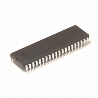
IC MCU 8MHZ 32K FLASH 40-DIP
Manufacturer
Freescale Semiconductor
Series
HC08r
Datasheet
1.MC68HC908GP32CFB.pdf
(410 pages)
Specifications of MC68HC908GP32CP
Core Processor
HC08
Core Size
8-Bit
Speed
8MHz
Connectivity
SCI, SPI
Peripherals
LVD, POR, PWM
Number Of I /o
33
Program Memory Size
32KB (32K x 8)
Program Memory Type
FLASH
Ram Size
512 x 8
Voltage - Supply (vcc/vdd)
2.7 V ~ 5.5 V
Data Converters
A/D 8x8b
Oscillator Type
Internal
Operating Temperature
-40°C ~ 85°C
Package / Case
40-DIP (0.600", 15.24mm)
For Use With
M68EVB908GP32 - BOARD EVALUATION FOR HC908GP32
Lead Free Status / RoHS Status
Contains lead / RoHS non-compliant
Eeprom Size
-
Available stocks
Company
Part Number
Manufacturer
Quantity
Price
Company:

Part Number:
MC68HC908GP32CP
Manufacturer:
ROCKWELL
Quantity:
201
Part Number:
MC68HC908GP32CP
Manufacturer:
MOTOROLA/摩托罗拉
Quantity:
20 000


7.6.5 PLL VCO Range Select Register
MC68HC908GP32
MOTOROLA
NOTE:
NOTE:
•
MC68HC08GP32
Address:
PMRS may be called PVRS on other HC08 derivatives.
The PLL VCO range select register (PMRS) contains the programming
information required for the hardware configuration of the VCO.
VRS7–VRS0 — VCO Range Select Bits
The VCO range select bits have built-in protection such that they cannot
be written when the PLL is on (PLLON = 1) and such that the VCO clock
cannot be selected as the source of the base clock (BCS = 1) if the VCO
range select bits are all clear.
The PLL VCO range select register must be programmed correctly.
Incorrect programming can result in failure of the PLL to achieve lock.
Reset:
Read:
Write:
These read/write bits control the hardware center-of-range linear
multiplier L which, in conjunction with E (See
7.4.6 Programming the
controls the hardware center-of-range frequency, f
cannot be written when the PLLON bit in the PCTL is set. (See
Special Programming
range select register disables the PLL and clears the BCS bit in the
PLL control register (PCTL). (See
and
register to $40 for a default range multiply value of 64.
Figure 7-8. PLL VCO Range Select Register (PMRS)
7.4.7 Special Programming
—
$003A
VRS7
Bit 7
Rev. 6
0
Clock Generator Module (CGMC)
VRS6
6
1
VRS5
5
0
Exceptions.) A value of $00 in the VCO
PLL, and
VRS4
4
0
7.4.8 Base Clock Selector Circuit
Exceptions.). Reset initializes the
7.6.1 PLL Control
VRS3
3
0
Clock Generator Module (CGMC)
7.4.3 PLL
VRS2
2
0
VRS
. VRS7–VRS0
Register.),
CGMC Registers
VRS1
Circuits,
1
0
Technical Data
VRS0
Bit 0
7.4.7
0
129
Related parts for MC68HC908GP32CP
Image
Part Number
Description
Manufacturer
Datasheet
Request
R

Part Number:
Description:
Manufacturer:
Freescale Semiconductor, Inc
Datasheet:
Part Number:
Description:
Manufacturer:
Freescale Semiconductor, Inc
Datasheet:
Part Number:
Description:
Manufacturer:
Freescale Semiconductor, Inc
Datasheet:
Part Number:
Description:
Manufacturer:
Freescale Semiconductor, Inc
Datasheet:
Part Number:
Description:
Manufacturer:
Freescale Semiconductor, Inc
Datasheet:
Part Number:
Description:
Manufacturer:
Freescale Semiconductor, Inc
Datasheet:
Part Number:
Description:
Manufacturer:
Freescale Semiconductor, Inc
Datasheet:
Part Number:
Description:
Manufacturer:
Freescale Semiconductor, Inc
Datasheet:
Part Number:
Description:
Manufacturer:
Freescale Semiconductor, Inc
Datasheet:
Part Number:
Description:
Manufacturer:
Freescale Semiconductor, Inc
Datasheet:
Part Number:
Description:
Manufacturer:
Freescale Semiconductor, Inc
Datasheet:
Part Number:
Description:
Manufacturer:
Freescale Semiconductor, Inc
Datasheet:
Part Number:
Description:
Manufacturer:
Freescale Semiconductor, Inc
Datasheet:
Part Number:
Description:
Manufacturer:
Freescale Semiconductor, Inc
Datasheet:
Part Number:
Description:
Manufacturer:
Freescale Semiconductor, Inc
Datasheet: