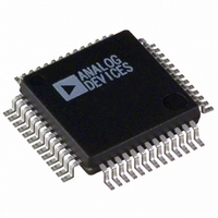
ADUC836BS Analog Devices Inc, ADUC836BS Datasheet - Page 66

ADUC836BS
Manufacturer Part Number
ADUC836BS
Description
IC ADC DUAL 16BIT W/MCU 52-MQFP
Manufacturer
Analog Devices Inc
Series
MicroConverter® ADuC8xxr
Datasheet
1.ADUC836BSZ.pdf
(80 pages)
Specifications of ADUC836BS
Rohs Status
RoHS non-compliant
Core Processor
8052
Core Size
8-Bit
Speed
12.58MHz
Connectivity
EBI/EMI, I²C, SPI, UART/USART
Peripherals
POR, PSM, PWM, Temp Sensor, WDT
Number Of I /o
34
Program Memory Size
62KB (62K x 8)
Program Memory Type
FLASH
Eeprom Size
4K x 8
Ram Size
2.25K x 8
Voltage - Supply (vcc/vdd)
2.7 V ~ 5.25 V
Data Converters
A/D 7x16b; D/A 1x12b
Oscillator Type
Internal
Operating Temperature
-40°C ~ 125°C
Package / Case
52-MQFP, 52-PQFP
Available stocks
Company
Part Number
Manufacturer
Quantity
Price
Company:
Part Number:
ADUC836BS
Manufacturer:
ADI
Quantity:
250
Part Number:
ADUC836BS
Manufacturer:
ADI/亚德诺
Quantity:
20 000
Company:
Part Number:
ADUC836BSZ
Manufacturer:
ADI
Quantity:
150
Company:
Part Number:
ADUC836BSZ
Manufacturer:
Analog Devices Inc
Quantity:
10 000
Part Number:
ADUC836BSZ
Manufacturer:
ADI/亚德诺
Quantity:
20 000
If the user plans to connect fast logic signals (rise/fall time < 5 ns)
to any of the ADuC836’s digital inputs, add a series resistor to
each relevant line to keep rise and fall times longer than 5 ns at the
ADuC836 input pins. A value of 100 or 200 is usually suf-
ficient to prevent high speed signals from coupling capacitively into
the ADuC836 and affecting the accuracy of ADC conversions.
ADuC836 System Self-Identification
In some hardware designs, it may be an advantage for the software
running on the ADuC836 target to identify the host MicroCon-
verter. For example, code running on the ADuC836 may also
be used with the ADuC824 or the ADuC816, and is required to
operate differently.
ADuC836
a.
b.
c.
Figure 64. System Grounding Schemes
PLACE ANALOG
COMPONENTS
PLACE ANALOG
COMPONENTS
HERE
PLACE ANALOG
AGND
AGND
COMPONENTS
HERE
HERE
GND
PLACE DIGITAL
COMPONENTS
PLACE DIGITAL
COMPONENTS
PLACE DIGITAL
COMPONENTS
HERE
HERE
HERE
DGND
DGND
–66–
The CHIPID SFR is a read-only register located at SFR address
C2H.The upper nibble of this SFR designates the MicroConverter
within the - ADC family. User software can read this SFR to
identify the host MicroConverter and thus execute slightly differ-
ent code if required. The CHIPID SFR reads as follows for the
- ADC family of MicroConverter products.
Clock Oscillator
As described earlier, the core clock frequency for the ADuC836
is generated from an on-chip PLL that locks onto a multiple (384
times) of 32.768 kHz. The latter is generated from an internal
clock oscillator. To use the internal clock oscillator, connect a
32.768 kHz parallel resonant crystal between the XTAL1 and
XTAL2 pins (32 and 33), as shown in Figure 65.
As shown in the typical external crystal connection diagram in
Figure 65, two internal 12 pF capacitors are provided on-chip.
These are connected internally, directly to the XTAL1 and
XTAL2 pins, and the total input capacitances at both pins is
detailed in the Specifications table. The value of the total load
capacitance required for the external crystal should be the value
recommended by the crystal manufacturer for use with that
specific crystal. In many cases, because of the on-chip capacitors,
additional external load capacitors will not be required.
To facilitate in-circuit programming plus in-circuit debug and
emulation options, users will want to implement some simple
connection points in their hardware that will allow easy access to
Download, Debug, and Emulation modes.
ADuC836
ADuC834
ADuC824
ADuC816
Figure 65. External Parallel Resonant Crystal
Connections Other Hardware Considerations
32.768kHz
XTAL2
XTAL1
32
33
12pF
12pF
ADuC836
CHIPID = 3xH
CHIPID = 2xH
CHIPID = 0xH
CHIPID = 1xH
TO INTERNAL
PLL
REV. A


