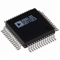
ADUC836BS Analog Devices Inc, ADUC836BS Datasheet - Page 11

ADUC836BS
Manufacturer Part Number
ADUC836BS
Description
IC ADC DUAL 16BIT W/MCU 52-MQFP
Manufacturer
Analog Devices Inc
Series
MicroConverter® ADuC8xxr
Datasheet
1.ADUC836BSZ.pdf
(80 pages)
Specifications of ADUC836BS
Rohs Status
RoHS non-compliant
Core Processor
8052
Core Size
8-Bit
Speed
12.58MHz
Connectivity
EBI/EMI, I²C, SPI, UART/USART
Peripherals
POR, PSM, PWM, Temp Sensor, WDT
Number Of I /o
34
Program Memory Size
62KB (62K x 8)
Program Memory Type
FLASH
Eeprom Size
4K x 8
Ram Size
2.25K x 8
Voltage - Supply (vcc/vdd)
2.7 V ~ 5.25 V
Data Converters
A/D 7x16b; D/A 1x12b
Oscillator Type
Internal
Operating Temperature
-40°C ~ 125°C
Package / Case
52-MQFP, 52-PQFP
Available stocks
Company
Part Number
Manufacturer
Quantity
Price
Company:
Part Number:
ADUC836BS
Manufacturer:
ADI
Quantity:
250
Part Number:
ADUC836BS
Manufacturer:
ADI/亚德诺
Quantity:
20 000
Company:
Part Number:
ADUC836BSZ
Manufacturer:
ADI
Quantity:
150
Company:
Part Number:
ADUC836BSZ
Manufacturer:
Analog Devices Inc
Quantity:
10 000
Part Number:
ADUC836BSZ
Manufacturer:
ADI/亚德诺
Quantity:
20 000
Pin No. Pin No.
52-Lead 56-Lead
MQFP
5
6
7
8
13
14
15
16–19,
22–25
20, 34, 48 22, 36, 51, DV
21, 35, 47 23, 37, 38, DGND
26
27
28–31
36–39
32
33
REV. A
CSP
4, 5
6, 7, 8
9
10
15
16
17
18–21,
24–27
50
30–33
39–42
34
35
Mnemonic
P1.4/AIN1
P1.5/AIN2
P1.6/AIN3
P1.7/AIN4/DAC
AV
AGND
REFIN(–)
REFIN(+)
SS
MISO
RESET
P3.0–P3.7
P3.0/RXD
P3.1/TXD
P3.2/INT0
P3.3/INT1
P3.4/T0/PWMCLK I/O
P3.5/T1
P3.6/WR
P3.7/RD
SCLOCK
MOSI/SDATA
P2.0–P2.7
(A8–A15)
(A16–A23)
XTAL1
XTAL2
DD
DD
Type* Description
I
I
I
I/O
S
S
I
I
I
I/O
I
I/O
I/O
I/O
I/O
I/O
I/O
I/O
I/O
S
S
I/O
I/O
I/O
I
O
PIN FUNCTION DESCRIPTIONS (continued)
and middle and high order address bytes during accesses to the 24-bit external data
Primary ADC, Positive Analog Input
Primary ADC, Negative Analog Input
Auxiliary ADC Input or Muxed Primary ADC, Positive Analog Input
Auxiliary ADC Input or Muxed Primary ADC, Negative Analog Input. The voltage
output from the DAC can also be configured to appear at this pin.
Analog Supply Voltage, 3 V or 5 V
Analog Ground. Ground reference pin for the analog circuitry.
Reference Input, Negative Terminal
Reference Input, Positive Terminal
Slave Select Input for the SPI Interface. A weak pull-up is present on this pin.
Master Input/Slave Output for the SPI Interface. A weak pull-up is present on this input pin.
Reset Input. A high level on this pin for 16 core clock cycles while the oscillator is
running resets the device. There is an internal weak pull-down and a Schmitt trigger
input stage on this pin.
P3.0–P3.7 are bidirectional port pins with internal pull-up resistors. Port 3 pins that
have 1s written to them are pulled high by the internal pull-up resistors, and in that
state can be used as inputs. As inputs, Port 3 pins being pulled externally low will
source current because of the internal pull-up resistors. When driving a 0-to-1 output
transition, a strong pull-up is active for two core clock periods of the instruction
cycle. Port 3 pins also have various secondary functions including:
Receiver Data for UART Serial Port
Transmitter Data for UART Serial Port
External Interrupt 0. This pin can also be used as a gate control input to Timer 0.
External Interrupt 1. This pin can also be used as a gate control input to Timer 1.
Timer/Counter 0 External Input. If the PWM is enabled, an external clock may be
input at this pin.
Timer/Counter 1 External Input
External Data Memory Write Strobe. Latches the data byte from Port 0 into an
external data memory.
External Data Memory Read Strobe. Enables the data from an external data memory
to Port 0.
Digital Supply, 3 V or 5 V
Digital Ground. Ground reference point for the digital circuitry.
Serial Interface Clock for either the I
Schmitt-triggered input, and a weak internal pull-up is present on this pin unless it is
outputting logic low. This pin can also be directly controlled in software as a digital
output pin.
Serial Data I/O for the I
SPI Interface. A weak internal pull-up is present on this pin unless it is outputting
logic low. This pin can also be directly controlled in software as a digital output pin.
Port 2 is a bidirectional port with internal pull-up resistors. Port 2 pins that have 1s
written to them are pulled high by the internal pull-up resistors, and in that state can
be used as inputs. As inputs, Port 2 pins being pulled externally low will source current
because of the internal pull-up resistors.
Port 2 emits the high order address bytes during fetches from external program memory
memory space.
Input to the Crystal Oscillator Inverter
Output from the Crystal Oscillator Inverter. (See the Hardware Design Considerations
section for description.)
–11–
2
C Interface or Master Output/Slave Input for the
2
C or SPI Interface. As an input, this pin is a
ADuC836


