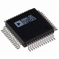
ADUC836BS Analog Devices Inc, ADUC836BS Datasheet - Page 39

ADUC836BS
Manufacturer Part Number
ADUC836BS
Description
IC ADC DUAL 16BIT W/MCU 52-MQFP
Manufacturer
Analog Devices Inc
Series
MicroConverter® ADuC8xxr
Datasheet
1.ADUC836BSZ.pdf
(80 pages)
Specifications of ADUC836BS
Rohs Status
RoHS non-compliant
Core Processor
8052
Core Size
8-Bit
Speed
12.58MHz
Connectivity
EBI/EMI, I²C, SPI, UART/USART
Peripherals
POR, PSM, PWM, Temp Sensor, WDT
Number Of I /o
34
Program Memory Size
62KB (62K x 8)
Program Memory Type
FLASH
Eeprom Size
4K x 8
Ram Size
2.25K x 8
Voltage - Supply (vcc/vdd)
2.7 V ~ 5.25 V
Data Converters
A/D 7x16b; D/A 1x12b
Oscillator Type
Internal
Operating Temperature
-40°C ~ 125°C
Package / Case
52-MQFP, 52-PQFP
Available stocks
Company
Part Number
Manufacturer
Quantity
Price
Company:
Part Number:
ADUC836BS
Manufacturer:
ADI
Quantity:
250
Part Number:
ADUC836BS
Manufacturer:
ADI/亚德诺
Quantity:
20 000
Company:
Part Number:
ADUC836BSZ
Manufacturer:
ADI
Quantity:
150
Company:
Part Number:
ADUC836BSZ
Manufacturer:
Analog Devices Inc
Quantity:
10 000
Part Number:
ADUC836BSZ
Manufacturer:
ADI/亚德诺
Quantity:
20 000
ON-CHIP PLL
The ADuC836 is intended for use with a 32.768 kHz watch
crystal. A PLL locks onto a multiple (384) of this to provide a
stable 12.582912 MHz clock for the system. The core can
operate at this frequency, or at binary submultiples of it, to allow
power saving in cases where maximum core performance is not
PLLCON
SFR Address
Power-On Default Value
Bit Addressable
Bit
7
6
5
4
3
2
1
0
REV. A
Name
OSC_PD
LOCK
–––
LTEA
FINT
CD2
CD1
CD0
Description
Oscillator Power-Down Bit.
Set by user to halt the 32 kHz oscillator in Power-Down mode.
Cleared by user to enable the 32 kHz oscillator in Power-Down mode.
This feature allows the TIC to continue counting even in Power-Down mode.
PLL Lock Bit. This is a read-only bit.
Set automatically at power-on to indicate the PLL loop is correctly tracking the crystal clock. After
power-down, this bit can be polled to wait for the PLL to lock.
Cleared automatically at power-on to indicate the PLL is not correctly tracking the crystal clock. This may
be due to the absence of a crystal clock or an external crystal at power-on. In this mode, the PLL output
can be 12.58 MHz ± 20%. After the ADuC836 wakes up from power-down, user code may poll this bit
to wait for the PLL to lock. If LOCK = 0, then the PLL is not locked.
Reserved for Future Use. Should be written with 0.
Reading this bit returns the state of the external EA pin latched at reset or power-on.
Fast Interrupt Response Bit.
Set by user enabling the response to any interrupt to be executed at the fastest core clock frequency,
regardless of the configuration of the CD2–0 bits (see below). After user code has returned from an interrupt,
the core resumes code execution at the core clock selected by the CD2–0 bits. Cleared by user to disable
the fast interrupt response feature.
CPU (Core Clock) Divider Bits.
This number determines the frequency at which the microcontroller core will operate.
CD2
0
0
0
0
1
1
1
1
PLL Control Register
D7H
03H
No
CD1
0
0
1
1
0
0
1
1
Table XVII. PLLCON SFR Bit Designations
CD0
0
1
0
1
0
1
0
1
Core Clock Frequency (MHz)
12.582912
6.291456
3.145728
1.572864 (Default Core Clock Frequency)
0.786432
0.393216
0.196608
0.098304
–39–
required. The default core clock is the PLL clock divided by
8 or 1.572864 MHz. The ADC clocks are also derived from the
PLL clock, with the modulator rate being the same as the crystal
oscillator frequency. This choice of frequencies ensures that the
modulators and the core will be synchronous, regardless of the
core clock rate. The PLL control register is PLLCON.
ADuC836


