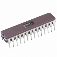
PIC16C745/JW Microchip Technology, PIC16C745/JW Datasheet - Page 96

PIC16C745/JW
Manufacturer Part Number
PIC16C745/JW
Description
IC MCU EPROM8KX14 USB A/D 28CDIP
Manufacturer
Microchip Technology
Series
PIC® 16Cr
Datasheets
1.PIC16F616T-ISL.pdf
(8 pages)
2.PIC16C745-ISP.pdf
(165 pages)
3.PIC16C745-ISP.pdf
(6 pages)
4.PIC16C745-ISP.pdf
(6 pages)
Specifications of PIC16C745/JW
Core Processor
PIC
Core Size
8-Bit
Speed
24MHz
Connectivity
SCI, UART/USART, USB
Peripherals
Brown-out Detect/Reset, POR, PWM, WDT
Number Of I /o
22
Program Memory Size
14KB (8K x 14)
Program Memory Type
EPROM, UV
Ram Size
256 x 8
Voltage - Supply (vcc/vdd)
4.35 V ~ 5.25 V
Data Converters
A/D 5x8b
Oscillator Type
External
Operating Temperature
0°C ~ 70°C
Package / Case
28-CDIP (0.300", 7.62mm) Window
Lead Free Status / RoHS Status
Contains lead / RoHS non-compliant
Eeprom Size
-
Available stocks
Company
Part Number
Manufacturer
Quantity
Price
Company:
Part Number:
PIC16C745/JW
Manufacturer:
MICROCHIP
Quantity:
51
Part Number:
PIC16C745/JW
Manufacturer:
MICROCHIP/微芯
Quantity:
20 000
PIC16C745/765
12.2
The A/D conversion time per bit is defined as T
A/D conversion requires 9.5T
The source of the A/D conversion clock is software
selectable. The four possible options for T
For correct A/D conversions, the A/D conversion clock
(T
of 1.6 s.
TABLE 12-1:
12.3
The ADCON1, TRISA and TRISE registers control the
operation of the A/D port pins. The port pins that are
desired as analog inputs must have their correspond-
ing TRIS bits set (input). If the TRIS bit is cleared (out-
put), the digital output level (V
converted.
The A/D operation is independent of the state of the
CHS<2:0> bits and the TRIS bits.
DS41124C-page 96
2T
8T
32T
RC
Note 1: The RC source has a typical T
AD
Operation
Note 1: When reading the port register, all pins
OSC
OSC
) must be selected to ensure a minimum T
• 2T
• 8T
• 32T
• Dedicated Internal RC oscillator
OSC
AD Clock Source (T
2: For device frequencies above 1 MHz, the
2: Analog levels on any pin that is defined as
3: The TRISE register is not provided on the
Selecting the A/D Conversion Clock
Configuring Analog Port Pins
OSC
OSC
device must be in SLEEP for the entire con-
version, or the A/D accuracy may be out of
specification.
OSC
configured as analog input channels will
read as cleared (a low level). Pins config-
ured as digital inputs will convert an ana-
log input. Analog levels on a digitally
configured input will not affect the conver-
sion accuracy.
a digital input, but not as an analog input,
may cause the input buffer to consume
current that is out of specification.
PIC16C745.
00
01
10
11
ADCS1:ADCS0
T
FREQUENCIES
AD
vs. DEVICE OPERATING
AD
)
AD
per 8-bit conversion.
OH
83.3 ns
333.3 ns
1.333
2 - 6 s
or V
Frequency
AD
24 MHz
Device
AD
time of 4 s.
OL
(1,2)
are:
) will be
AD
AD
. The
time
Preliminary
12.4
Clearing the GO/DONE bit during a conversion will
abort the current conversion. The ADRES register will
NOT be updated with the partially completed A/D con-
version sample. That is, the ADRES register will con-
tinue to contain the value of the last completed
conversion (or the last value written to the ADRES reg-
ister). After the A/D conversion is aborted, a 2T
is required before the next acquisition is started. After
this 2T
the selected channel.
12.5
The A/D module can operate during SLEEP mode.
This requires that the A/D clock source be set to RC
(ADCS<1:0> = 11). When the RC clock source is
selected, the A/D module waits one instruction cycle
before starting the conversion. This allows the SLEEP
instruction to be executed, which eliminates all digital
switching noise from the conversion. When the con-
version is completed, the GO/DONE bit will be
cleared, and the result loaded into the ADRES regis-
ter. If the A/D interrupt is enabled, the device will
wake-up from SLEEP. If the A/D interrupt is not
enabled, the A/D module will then be turned off,
although the ADON bit will remain set.
When the A/D clock source is another clock option (not
RC), a SLEEP instruction will cause the present conver-
sion to be aborted and the A/D module to be turned off,
though the ADON bit will remain set.
Turning off the A/D places the A/D module in its lowest
current consumption state.
12.6
A device RESET forces all registers to their RESET
state. The A/D module is disabled and any conversion
in progress is aborted. All pins with analog functions
are configured as available inputs.
The ADRES register will contain unknown data after a
Power-on Reset.
Note:
Note:
AD
A/D Conversions
A/D Operation During Sleep
Effects of a RESET
wait, an acquisition is automatically started on
The GO/DONE bit should NOT be set in
the same instruction that turns on the A/D.
For the A/D module to operate in SLEEP,
the A/D clock source must be set to RC
(ADCS<1:0> = 11). To perform an A/D
conversion in SLEEP, ensure the SLEEP
instruction immediately follows the instruc-
tion that sets the GO/DONE bit.
2000 Microchip Technology Inc.
AD
wait


