PIC16C745/JW Microchip Technology, PIC16C745/JW Datasheet - Page 157
PIC16C745/JW
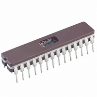
Manufacturer Part Number
PIC16C745/JW
Description
IC MCU EPROM8KX14 USB A/D 28CDIP
Manufacturer
Microchip Technology
Series
PIC® 16Cr
Datasheets
1.PIC16F616T-ISL.pdf
(8 pages)
2.PIC16C745-ISP.pdf
(165 pages)
3.PIC16C745-ISP.pdf
(6 pages)
4.PIC16C745-ISP.pdf
(6 pages)
Specifications of PIC16C745/JW
Core Processor
PIC
Core Size
8-Bit
Speed
24MHz
Connectivity
SCI, UART/USART, USB
Peripherals
Brown-out Detect/Reset, POR, PWM, WDT
Number Of I /o
22
Program Memory Size
14KB (8K x 14)
Program Memory Type
EPROM, UV
Ram Size
256 x 8
Voltage - Supply (vcc/vdd)
4.35 V ~ 5.25 V
Data Converters
A/D 5x8b
Oscillator Type
External
Operating Temperature
0°C ~ 70°C
Package / Case
28-CDIP (0.300", 7.62mm) Window
Lead Free Status / RoHS Status
Contains lead / RoHS non-compliant
Eeprom Size
-
Available stocks
Company
Part Number
Manufacturer
Quantity
Price
Company:

Part Number:
PIC16C745/JW
Manufacturer:
MICROCHIP
Quantity:
51
Part Number:
PIC16C745/JW
Manufacturer:
MICROCHIP/微芯
Quantity:
20 000


INDEX
A
A/D
Absolute Maximum Ratings ............................................. 127
ADRES Register ......................................................... 17
Application Notes
Architecture
Assembler
B
Baud Rate Formula ........................................................... 79
Block Diagrams
BOR bit ............................................................................ 103
BRGH bit ........................................................................... 79
Brown-out Reset (BOR)
Buffer Descriptor Table ...................................................... 68
2000 Microchip Technology Inc.
ADCON0 Register ..................................................... 91
Analog Input Model Block Diagram ........................... 95
Analog-to-Digital Converter ....................................... 91
Block Diagram ........................................................... 94
Configuring Analog Port Pins .................................... 96
Configuring the Interrupt ............................................ 94
Configuring the Module ............................................. 94
Conversion Clock ...................................................... 96
Conversions .............................................................. 96
Converter Characteristics ........................................ 141
Effects of a Reset ...................................................... 96
Faster Conversion - Lower Resolution Tradeoff ........ 96
Internal Sampling Switch (Rss) Impedance ................ 95
Operation During Sleep ............................................. 96
Sampling Requirements ............................................ 95
Source Impedance .................................................... 95
Timing Diagram ....................................................... 142
Using the CCP Trigger .............................................. 97
AN552 (Implementing Wake-up on Key Strokes
Using PIC16CXXX) ................................................... 33
AN556 (Table Reading Using PIC16CXX ................. 29
AN607, Power-up Trouble Shooting ........................ 103
Overview ..................................................................... 9
MPASM Assembler ................................................. 121
A/D ............................................................................ 94
Analog Input Model ................................................... 95
Capture ...................................................................... 53
Compare .................................................................... 54
On-Chip Reset Circuit ............................................. 102
PORTC ...................................................................... 35
PORTD (In I/O Port Mode) ........................................ 37
PORTD and PORTE as a Parallel Slave Port ........... 40
PORTE (In I/O Port Mode) ........................................ 38
PWM .......................................................................... 54
RA4/T0CKI Pin .......................................................... 31
RB Port Pins .............................................................. 33
RB Port Pins .............................................................. 33
Timer0/WDT Prescaler .............................................. 43
Timer2 ....................................................................... 49
USART Receive ........................................................ 83
USART Transmit ....................................................... 81
Watchdog Timer ...................................................... 110
Timing Diagram ....................................................... 136
,
Preliminary
91
C
C bit ................................................................................... 22
Capture/Compare/PWM
Capture/Compare/PWM (CCP)
CCP1CON ......................................................................... 19
CCP2CON ......................................................................... 19
CCPR1H Register ............................................... 17
CCPR1L Register ....................................................... 19
CCPR2H Register ...................................................... 17
CCPR2L Register ....................................................... 17
Clocking Scheme .............................................................. 13
Code Examples
Code Protection ....................................................... 99
Computed GOTO .............................................................. 29
Configuration Bits .............................................................. 99
Control ............................................................................... 60
CREN bit ........................................................................... 78
CS pin ............................................................................... 40
D
DC bit ................................................................................ 22
DC Characteristics ................................................. 129
Development Support ................................................ 5
Direct Addressing .............................................................. 30
E
EC Oscillator ................................................................... 104
Electrical Characteristics ................................................. 127
Endpoint ............................................................................ 71
Errata .................................................................................. 3
Error .................................................................................. 63
F
FERR bit ............................................................................ 78
FSR Register ................................................ 17
G
General Description ............................................................ 5
GIE bit ............................................................................. 107
Capture
CCP Timer Resources .............................................. 51
Compare
Interaction of Two CCP Modules .............................. 51
Section ...................................................................... 51
Special Event Trigger and A/D Conversions ............. 54
PWM Block Diagram ................................................. 54
PWM Mode ............................................................... 54
Timing Diagram ....................................................... 138
Call of a Subroutine in Page 1 from Page 0 .............. 29
Changing Prescaler (Timer0 to WDT) ....................... 44
Indirect Addressing ................................................... 30
Initializing PORTA ..................................................... 31
Block Diagram ................................................... 53
CCP1CON Register .......................................... 52
CCP1IF ............................................................. 53
Mode ................................................................. 53
Prescaler ........................................................... 53
Block Diagram ................................................... 54
Mode ................................................................. 54
Software Interrupt Mode ................................... 54
Special Event Trigger ........................................ 54
Special Trigger Output of CCP1 ....................... 54
Special Trigger Output of CCP2 ....................... 54
PIC16C745/765
DS41124C-page 157
,
18
,
,
19
20
,
,
,
,
,
,
,
,
112
130
121
51
51
19
19
30
Related parts for PIC16C745/JW
Image
Part Number
Description
Manufacturer
Datasheet
Request
R

Part Number:
Description:
MICRO CTRL 4K 4MHZ OTP 44PLCC
Manufacturer:
Microchip Technology
Datasheet:
Part Number:
Description:
MICRO CTRL 4K 20MHZ OTP 44PLCC
Manufacturer:
Microchip Technology
Datasheet:

Part Number:
Description:
MICRO CTRL 4K 20MHZ OTP 40DIP
Manufacturer:
Microchip Technology
Datasheet:
Part Number:
Description:
MICRO CTRL 4K 10MHZ OTP ET 40DIP
Manufacturer:
Microchip Technology
Datasheet:
Part Number:
Description:
MICRO CTRL 4K 10MHZ OTP 40DIP
Manufacturer:
Microchip Technology
Datasheet:
Part Number:
Description:
MICRO CTRL 4K 4MHZ OTP 40DIP
Manufacturer:
Microchip Technology
Datasheet:
Part Number:
Description:
MICRO CTRL 4K 4MHZ OTP 40DIP
Manufacturer:
Microchip Technology
Datasheet:

Part Number:
Description:
MICRO CTRL 4K 20MHZ EPROM 40CDIP
Manufacturer:
Microchip Technology
Datasheet:

Part Number:
Description:
8-Bit CMOS Microcontrollers with A/D Converter
Manufacturer:
Microchip Technology
Part Number:
Description:
8-Bit CMOS Microcontrollers with A/D Converter
Manufacturer:
Microchip Technology
Part Number:
Description:
8-Bit CMOS Microcontrollers with A/D Converter
Manufacturer:
Microchip Technology
Part Number:
Description:
8-Bit CMOS Microcontrollers with A/D Converter
Manufacturer:
Microchip Technology
Part Number:
Description:
8-Bit CMOS Microcontrollers with A/D Converter
Manufacturer:
Microchip Technology
Part Number:
Description:
8-Bit CMOS Microcontrollers with A/D Converter
Manufacturer:
Microchip Technology
Part Number:
Description:
8-Bit CMOS Microcontrollers with A/D Converter
Manufacturer:
Microchip Technology