PIC16C745/JW Microchip Technology, PIC16C745/JW Datasheet - Page 9
PIC16C745/JW
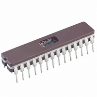
Manufacturer Part Number
PIC16C745/JW
Description
IC MCU EPROM8KX14 USB A/D 28CDIP
Manufacturer
Microchip Technology
Series
PIC® 16Cr
Datasheets
1.PIC16F616T-ISL.pdf
(8 pages)
2.PIC16C745-ISP.pdf
(165 pages)
3.PIC16C745-ISP.pdf
(6 pages)
4.PIC16C745-ISP.pdf
(6 pages)
Specifications of PIC16C745/JW
Core Processor
PIC
Core Size
8-Bit
Speed
24MHz
Connectivity
SCI, UART/USART, USB
Peripherals
Brown-out Detect/Reset, POR, PWM, WDT
Number Of I /o
22
Program Memory Size
14KB (8K x 14)
Program Memory Type
EPROM, UV
Ram Size
256 x 8
Voltage - Supply (vcc/vdd)
4.35 V ~ 5.25 V
Data Converters
A/D 5x8b
Oscillator Type
External
Operating Temperature
0°C ~ 70°C
Package / Case
28-CDIP (0.300", 7.62mm) Window
Lead Free Status / RoHS Status
Contains lead / RoHS non-compliant
Eeprom Size
-
Available stocks
Company
Part Number
Manufacturer
Quantity
Price
Company:

Part Number:
PIC16C745/JW
Manufacturer:
MICROCHIP
Quantity:
51
Part Number:
PIC16C745/JW
Manufacturer:
MICROCHIP/微芯
Quantity:
20 000


3.0
The high performance of the PIC16C745/765 family
can be attributed to a number of architectural features
commonly found in RISC microprocessors. To begin
with, the PIC16C745/765 uses a Harvard architecture,
in which program and data are accessed from separate
memories using separate buses. This improves band-
width over traditional von Neumann architecture in
which program and data are fetched from the same
memory using the same bus. Separating program and
data buses further allows instructions to be sized differ-
ently than the 8-bit wide data word. Instruction opcodes
are 14-bits wide making it possible to have all single
word instructions. A 14-bit wide program memory
access bus fetches a 14-bit instruction in a single cycle.
A two-stage pipeline overlaps fetch and execution of
instructions
instructions execute in a single cycle (166.6667 ns @
24 MHz) except for program branches.
The PIC16C745/765 can directly or indirectly address
its register files or data memory. All special function
registers, including the program counter, are mapped in
the data memory. The PIC16C745/765 has an orthog-
onal (symmetrical) instruction set that makes it possible
to carry out any operation on any register using any
addressing mode. This symmetrical nature and lack of
‘special optimal situations’ make programming with the
PIC16C745/765 simple yet efficient. In addition, the
learning curve is reduced significantly.
Device
PIC16C745
PIC16C765
2000 Microchip Technology Inc.
ARCHITECTURAL OVERVIEW
Program
(Example 3-1).
x14
8K
8K
Memory
Data
256
256
x8
Pins
28
40
Consequently,
Resolution
A/D
8
8
Channels
A/D
most
5
8
Preliminary
PIC16C745/765 devices contain an 8-bit ALU and
working register. The ALU is a general purpose arith-
metic unit. It performs arithmetic and Boolean functions
between the data in the working register and any regis-
ter file.
The ALU is 8-bits wide and capable of addition, sub-
traction, shift and logical operations. Unless otherwise
mentioned, arithmetic operations are two's comple-
ment in nature. In two-operand instructions, typically
one operand is the working register (W register). The
other operand is a file register or an immediate con-
stant. In single operand instructions, the operand is
either the W register or a file register.
The W register is an 8-bit working register used for ALU
operations. It is not an addressable register.
Depending on the instruction executed, the ALU may
affect the values of the Carry (C), Digit Carry (DC), and
Zero (Z) bits in the STATUS register. The C and DC bits
operate as a borrow bit and a digit borrow out bit,
respectively, in subtraction. See the SUBLW and SUBWF
instructions for examples.
PIC16C745/765
DS41124C-page 9
Related parts for PIC16C745/JW
Image
Part Number
Description
Manufacturer
Datasheet
Request
R

Part Number:
Description:
MICRO CTRL 4K 4MHZ OTP 44PLCC
Manufacturer:
Microchip Technology
Datasheet:
Part Number:
Description:
MICRO CTRL 4K 20MHZ OTP 44PLCC
Manufacturer:
Microchip Technology
Datasheet:

Part Number:
Description:
MICRO CTRL 4K 20MHZ OTP 40DIP
Manufacturer:
Microchip Technology
Datasheet:
Part Number:
Description:
MICRO CTRL 4K 10MHZ OTP ET 40DIP
Manufacturer:
Microchip Technology
Datasheet:
Part Number:
Description:
MICRO CTRL 4K 10MHZ OTP 40DIP
Manufacturer:
Microchip Technology
Datasheet:
Part Number:
Description:
MICRO CTRL 4K 4MHZ OTP 40DIP
Manufacturer:
Microchip Technology
Datasheet:
Part Number:
Description:
MICRO CTRL 4K 4MHZ OTP 40DIP
Manufacturer:
Microchip Technology
Datasheet:

Part Number:
Description:
MICRO CTRL 4K 20MHZ EPROM 40CDIP
Manufacturer:
Microchip Technology
Datasheet:

Part Number:
Description:
8-Bit CMOS Microcontrollers with A/D Converter
Manufacturer:
Microchip Technology
Part Number:
Description:
8-Bit CMOS Microcontrollers with A/D Converter
Manufacturer:
Microchip Technology
Part Number:
Description:
8-Bit CMOS Microcontrollers with A/D Converter
Manufacturer:
Microchip Technology
Part Number:
Description:
8-Bit CMOS Microcontrollers with A/D Converter
Manufacturer:
Microchip Technology
Part Number:
Description:
8-Bit CMOS Microcontrollers with A/D Converter
Manufacturer:
Microchip Technology
Part Number:
Description:
8-Bit CMOS Microcontrollers with A/D Converter
Manufacturer:
Microchip Technology
Part Number:
Description:
8-Bit CMOS Microcontrollers with A/D Converter
Manufacturer:
Microchip Technology