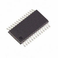
MAXQ3108-FFN+ Maxim Integrated Products, MAXQ3108-FFN+ Datasheet - Page 17

MAXQ3108-FFN+
Manufacturer Part Number
MAXQ3108-FFN+
Description
IC MCU DUAL-CORE 16BIT 28-TSSOP
Manufacturer
Maxim Integrated Products
Series
MAXQ™r
Datasheet
1.MAXQ3108-FFN.pdf
(64 pages)
Specifications of MAXQ3108-FFN+
Core Processor
RISC
Core Size
16-Bit
Speed
10MHz
Connectivity
I²C, SPI, UART/USART
Peripherals
POR, PWM, WDT
Number Of I /o
21
Program Memory Size
64KB (32K x 16)
Program Memory Type
FLASH
Ram Size
11K x 8
Voltage - Supply (vcc/vdd)
1.8 V ~ 3.6 V
Oscillator Type
External
Operating Temperature
-40°C ~ 85°C
Package / Case
28-TSSOP
Processor Series
MAXQ
Core
RISC
Data Bus Width
16 bit
Data Ram Size
2 KB
Interface Type
I2C, JTAG, SPI
Maximum Clock Frequency
10 MHz
Number Of Programmable I/os
22
Number Of Timers
2
Operating Supply Voltage
3.6 V
Maximum Operating Temperature
+ 85 C
Mounting Style
SMD/SMT
Minimum Operating Temperature
- 40 C
Lead Free Status / RoHS Status
Lead free / RoHS Compliant
Eeprom Size
-
Data Converters
-
Lead Free Status / Rohs Status
Lead free / RoHS Compliant
AD0 (00h, 00h)
Initialization:
Read/Write Access:
AD0.[15:0]:
AD1 (01h, 00h)
AD2 (02h, 00h)
AD3 (03h, 00h)
AD4 (04h, 00h)
AD5 (05h, 00h)
SRSP0 (06h, 00h)
Initialization:
Read/Write Access:
SRSP0.[3:0]: RSPST[3:0]
SRSP0.4: REQE
SRSP0.5: RSPSDV
SRSP0.[7:6]: Reserved
REGISTER
______________________________________________________________________________________
Low-Power, Dual-Core Microcontroller
Analog-to-Digital Converter 0 Output Register
This register is reset to 0xFFFF on all forms of reset.
Unrestricted read access.
Analog-to-Digital Converter 0 Output Register. This register contains the most significant 16 bits
of the current ADC0 data sample that was acquired from the respective sinc3 filter. Reading from
the ADC0 register(s) results in the ABF0 flag being cleared by hardware (when set), unless the read
operation is performed simultaneously with a write. Reading a disabled ADC returns the data last
acquired if the associated buffer full flag is set and returns FFFFh if the flag is clear.
Analog-to-Digital Converter 1 Output Register
Analog-to-Digital Converter 2 Output Register
Analog-to-Digital Converter 3 Output Register
Analog-to-Digital Converter 4 Output Register
Analog-to-Digital Converter 5 Output Register
Slave Response Register 0
This register is reset to 00h on all forms of reset.
Unrestricted read access only to the UserCore (except RSPSDV; see the bit description).
Unrestricted read/write access to the DSPCore (except RSPSDV and RSPST[3:0]; see the bit
descriptions).
Response Status Bits 3:0. These bits can be used to report acknowledgement and status of the
current command being processed by the slave and to report slave system conditions (e.g.,
watchdog timeout) that are not related to a master command. To notify the master that status is
ready to be read, the RSP0DV bit should be set to 1 either by software (in the case of command
status) or, in some cases, by hardware (as for the watchdog). In cases where slave hardware sets
the status bits, these bits are not writable by slave software until the status condition has been
cleared.
When the DSPCore watchdog timer reaches FFFFh, a system interrupt from the DSPCore is signaled
by the setting of the SRSP0.5 status flag along with the SRSP0.[3:0] status code of 0000b. This
hardware condition for the SRSP0 register persists (preventing software writes of these bits by the
DSPCore) until a reset of the DSPCore is executed (UserCore may disable the DSPCore through
ENDSP = 0 to force the reset).
Request Registers Interrupt Enable. Setting this bit to 1 enables an interrupt for the master
request-command data valid (interrupt) flag (REQCDV). The master request-command data valid
flag is reported in MREQ0.5 (and the associated command code is contained in MREQ0.[3:0]).
Clearing this bit to 0 disables the interrupt associated with the master request-command data valid
flag.
Response Status Data Valid Flag. This flag can only be set by the slave (DSPCore) or slave
hardware once a valid status or system interrupt condition is supplied in the RSPST[3:0] field of the
SRSP0 register to notify the master that valid status is ready for reading. Status information or data
could also be contained in SRSP1, so the slave should only set this flag when all data has been
loaded (included any that is loaded to SRSP1). This flag can only be cleared by the master
(UserCore) software unless the status condition that caused hardware to set the flag persists (e.g.,
slave watchdog counter timeout). If made available by the slaveCPU, more information can be
ascertained about the status by additional master request read commands.
Reserved. Reads return 0.
Special Function Register Bit Descriptions
DESCRIPTION
17


