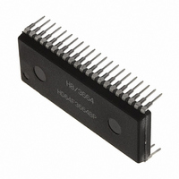
M38513E4FP#U0 Renesas Electronics America, M38513E4FP#U0 Datasheet - Page 63

M38513E4FP#U0
Manufacturer Part Number
M38513E4FP#U0
Description
IC 740 MCU ROM 16K 42SSOP
Manufacturer
Renesas Electronics America
Series
740/38000r
Specifications of M38513E4FP#U0
Core Processor
740
Core Size
8-Bit
Speed
8MHz
Connectivity
SIO, UART/USART
Peripherals
PWM, WDT
Number Of I /o
34
Program Memory Size
16KB (16K x 8)
Program Memory Type
OTP
Ram Size
512 x 8
Voltage - Supply (vcc/vdd)
2.7 V ~ 5.5 V
Data Converters
A/D 5x10b
Oscillator Type
External
Operating Temperature
-20°C ~ 85°C
Package / Case
42-SSOP
Package
42SSOP
Family Name
740
Maximum Speed
8 MHz
Operating Supply Voltage
5 V
Data Bus Width
8 Bit
Number Of Programmable I/os
34
Interface Type
I2C-BUS
On-chip Adc
5-chx10-bit
Number Of Timers
4
Lead Free Status / RoHS Status
Contains lead / RoHS non-compliant
Eeprom Size
-
3851 Group
(3) Standard serial I/O Mode
The standard serial I/O mode inputs and outputs the software
commands, addresses and data needed to operate (read, pro-
gram, erase, etc.) the internal flash memory. This I/O is clock
synchronized serial. This mode requires the exclusive external
equipment (serial programmer).
The standard serial I/O mode is different from the parallel I/O
mode in that the CPU controls flash memory rewrite (uses the
CPU rewrite mode), rewrite data input and so forth. The standard
serial I/O mode is started by connecting “H” to the P2
and “H” to the P4
V to 5.5 V to Vpp from an external source), and releasing the re-
set operation. (In the ordinary microcomputer mode, set CNVss
pin to “L” level.)
This control program is written in the Boot ROM area when the
product is shipped from Renesas Technology Corporation. Accord-
ingly, make note of the fact that the standard serial I/O mode
cannot be used if the Boot ROM area is rewritten in parallel I/O
mode. Figure 65 shows the pin connection for the standard serial
I/O mode.
In standard serial I/O mode, serial data I/O uses the four serial I/O
pins S
transfer clock input pin through which an external transfer clock is
input. The TxD pin is for CMOS output. The S
outputs “L” level when ready for reception and “H” level when re-
ception starts.
Serial data I/O is transferred serially in 8-bit units.
In standard serial I/O mode, only the User ROM area shown in
Figure 57 can be rewritten. The Boot ROM area cannot.
In standard serial I/O mode, a 7-byte ID code is used. When there
is data in the flash memory, commands sent from the peripheral
unit (programmer) are not accepted unless the ID code matches.
Rev.1.01
CLK1
, RxD, TxD and S
Oct 15, 2003
(Built-in 24 KB or more ROM)
1
(INT
0
) pin and “H” to the CNV
RDY1
page 61 of 89
(BUSY). The S
RDY1
SS
CLK1
pin (apply 4.5
6
(BUSY) pin
(S
pin is the
CLK1
) pin
Outline Performance (Standard Serial I/O
Mode)
In standard serial I/O mode, software commands, addresses and
data are input and output between the MCU and peripheral units
(serial programmer, etc.) using 4-wire clock-synchronized serial
I/O (serial I/O1).
In reception, software commands, addresses and program data
are synchronized with the rise of the transfer clock that is input to
the S
transmission, the read data and status are synchronized with the
fall of the transfer clock, and output from the TxD pin.
The TxD pin is for CMOS output. Transfer is in 8-bit units with LSB
first.
When busy, such as during transmission, reception, erasing or
program execution, the S
ingly, always start the next transfer after the S
“L” level.
Also, data and status registers in a memory can be read after in-
putting software commands. Status, such as the operating state of
the flash memory or whether a program or erase operation ended
successfully or not, can be checked by reading the status register.
Here following explains software commands, status registers, etc.
CLK1
pin, and are then input to the MCU via the RxD pin. In
RDY1
(BUSY) pin is “H” level. Accord-
RDY1
(BUSY) pin is


