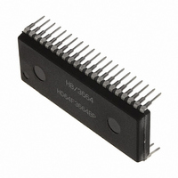
M38513E4FP#U0 Renesas Electronics America, M38513E4FP#U0 Datasheet - Page 31

M38513E4FP#U0
Manufacturer Part Number
M38513E4FP#U0
Description
IC 740 MCU ROM 16K 42SSOP
Manufacturer
Renesas Electronics America
Series
740/38000r
Specifications of M38513E4FP#U0
Core Processor
740
Core Size
8-Bit
Speed
8MHz
Connectivity
SIO, UART/USART
Peripherals
PWM, WDT
Number Of I /o
34
Program Memory Size
16KB (16K x 8)
Program Memory Type
OTP
Ram Size
512 x 8
Voltage - Supply (vcc/vdd)
2.7 V ~ 5.5 V
Data Converters
A/D 5x10b
Oscillator Type
External
Operating Temperature
-20°C ~ 85°C
Package / Case
42-SSOP
Package
42SSOP
Family Name
740
Maximum Speed
8 MHz
Operating Supply Voltage
5 V
Data Bus Width
8 Bit
Number Of Programmable I/os
34
Interface Type
I2C-BUS
On-chip Adc
5-chx10-bit
Number Of Timers
4
Lead Free Status / RoHS Status
Contains lead / RoHS non-compliant
Eeprom Size
-
3851 Group
MULTI-MASTER I
The multi-master I
cuit, conforming to the Philips I
interface, offering both arbitration lost detection and a synchronous
functions, is useful for the multi-master serial communications.
Figure 27 shows a block diagram of the multi-master I
terface and Table 9 lists the multi-master I
functions.
This multi-master I
register, the I
the I
condition control register and other control circuits.
When using the multi-master I
more to .
Note: Renesas Technology Corporation assumes no responsibility for in-
Fig. 27 Block diagram of multi-master I
Rev.1.01
: Purchase of Renesas Technology Corporation's I
system, provided that the system conforms to the I
2
C control register, the I
fringement of any third-party’s rights or originating in the use of the
connection control function between the I
ports SCL
ter (002E
Serial data
(SDA)
S2D
Serial
clock
(SCL)
Oct 15, 2003
SIS
2
16
1
C data shift register, the I
, SCL
(Built-in 24 KB or more ROM)
).
I
2
C start/stop condition
SIP
2
C-BUS interface is a serial communications cir-
2
2
C-BUS interface consists of the I
control register
, SDA
SSC4 SSC3 SSC2 SSC1 SSC0
2
Noise
elimination
circuit
Noise
elimination
circuit
C-BUS INTERFACE
1
and SDA
2
page 29 of 89
C status register, the I
2
2
C-BUS data transfer format. This
C-BUS interface, set 1 MHz or
2
with the bit 6 of I
Clock
control
circuit
2
C clock control register,
2
2
C-BUS interface
C-BUS interface and the
Data
control
circuit
circuit
circuit
2
2
2
C components conveys a license under the Philips I
AL
BB
C-BUS interface
C Standard Specification as defined by Philips.
2
C control regis-
S0D
2
I
2
C start/stop
2
b7
C clock control register
2
C address
SAD6 SAD5 SAD4 SAD3 SAD2 SAD1 SAD0 RWB
S2
C-BUS in-
ACK
b7
b7
S
0
ACK
BIT
I
Address comparator
2
MODE
I
FAST
C data shift register
2
C address register
CCR4 CCR3 CCR2 CCR1 CCR0
Clock division
Table 9 Multi-master I
SCL clock frequency
System clock
Communication mode
Format
Item
b0
b0
b0
System clock ( )
Internal data bus
= f(X
= f(X
2
C Patent Rights to use these components an I
IN
IN
MST TRX BB PIN
2
S1D I C control register
S1
b7
b7
TISS
C-BUS interface functions
)/2 (high-speed mode)
)/8 (middle-speed mode)
In conformity with Philips I
standard:
In conformity with Philips I
standard:
16.1 kHz to 400 kHz (at = 4 MHz)
10-bit addressing format
7-bit addressing format
High-speed clock mode
Standard clock mode
Master transmission
Master reception
Slave transmission
Slave reception
CLK
STP
2
Interrupt
generating
circuit
10BIT
SAD
I
2
ALS
C clock control register
ES0
Function
AL AAS AD0 LRB
I
2
C status register
Interrupt request signal
(IICIRQ)
BC2 BC1 BC0
S1D
Bit counter
2
2
C-BUS
C-BUS
b0
b0
2
C


