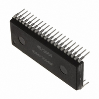
M38513E4FP#U0 Renesas Electronics America, M38513E4FP#U0 Datasheet - Page 5

M38513E4FP#U0
Manufacturer Part Number
M38513E4FP#U0
Description
IC 740 MCU ROM 16K 42SSOP
Manufacturer
Renesas Electronics America
Series
740/38000r
Specifications of M38513E4FP#U0
Core Processor
740
Core Size
8-Bit
Speed
8MHz
Connectivity
SIO, UART/USART
Peripherals
PWM, WDT
Number Of I /o
34
Program Memory Size
16KB (16K x 8)
Program Memory Type
OTP
Ram Size
512 x 8
Voltage - Supply (vcc/vdd)
2.7 V ~ 5.5 V
Data Converters
A/D 5x10b
Oscillator Type
External
Operating Temperature
-20°C ~ 85°C
Package / Case
42-SSOP
Package
42SSOP
Family Name
740
Maximum Speed
8 MHz
Operating Supply Voltage
5 V
Data Bus Width
8 Bit
Number Of Programmable I/os
34
Interface Type
I2C-BUS
On-chip Adc
5-chx10-bit
Number Of Timers
4
Lead Free Status / RoHS Status
Contains lead / RoHS non-compliant
Eeprom Size
-
Table 1 Pin description
3851 Group
Rev.1.01
V
CNV
V
AV
RESET
X
X
P0
P0
P0
P0
P0
P1
P2
P2
P2
P2
P2
P2
P2
P2
S
P3
P3
P4
P4
P4
P4
P4
CC
REF
IN
OUT
RDY1
0
1
2
3
4
0
0
1
2
3
4
5
6
7
0
4
0
1
2
3
4
SS
/S
/S
/AN
/AN
/INT
/INT
/INT
/INT
/S
/S
/S
–P0
–P1
/X
/X
/SDA
/SCL
/SDA
/SCL
/CNTR
/CNTR
, V
SS
IN2
OUT2
CLK2
RDY2
COUT
CIN
CLK1
Pin
SS
0
4
7
7
0
1
2
3
–
1
2
1
2
/S
/PWM
/TxD
/RxD
0
1
CMP2
Oct 15, 2003
/
(Built-in 24 KB or more ROM)
I/O port P0
I/O port P1
I/O port P2
I/O port P3
I/O port P4
Power source
CNV
Reference
voltage input
Analog power
source input
Reset input
Clock input
Clock output
SS
Name
input
page 3 of 89
•Apply voltage of 2.7 V – 5.5 V to Vcc, and 0 V to Vss.
•This pin controls the operation mode of the chip.
•Normally connected to V
•Reference voltage input pin for A-D converter.
•Analog power source input pin for A-D converter.
•Connect to Vss.
•Reset input pin for active “L”.
•Input and output pins for the clock generating circuit.
•Connect a ceramic resonator or quartz-crystal oscillator between the X
•When an external clock is used, connect the clock source to the X
•8-bit CMOS I/O port.
•I/O direction register allows each pin to be individually
•CMOS compatible input level.
•CMOS 3-state output structure.
•P1
•8-bit CMOS I/O port.
•I/O direction register allows each pin to be individually
•CMOS compatible input level.
•P2
•P2
•P2
•P2
•8-bit CMOS I/O port with the same function as port P0.
•CMOS compatible input level.
•CMOS 3-state output structure.
•8-bit CMOS I/O port with the same function as port P0.
•CMOS compatible input level.
•CMOS 3-state output structure.
the oscillation frequency.
pin open.
programmed as either input or output.
for LED drive.
programmed as either input or output.
input level or SMBUS input level in the I
face function.
BUS interface function.
2
0
2
0
4
, P2
, P2
, P2
to P2
to P1
1
3
5
, P2
: N-channel open-drain structure.
: N-channel open-drain structure in the I
5
7
can be switched between CMOS compatible
(8 bits) are enabled to output large current
4
to P2
7
: CMOS3-state output structure.
Functions
SS
.
2
C-BUS inter-
2
C-
• Serial I/O2 function pin
• Sub-clock generating circuit I/O
pins (connect a resonator)
• I
• I
Serial I/O1 function pins
• Serial I/O1 function pin
• Serial I/O1 function pin/Timer X
function pin
• A-D converter input pin
• Timer Y function pin
• Interrupt input pins
• Interrupt input pin
• S
• Interrupt input pin
• PWM output pin
2
2
Function except a port function
CMP2
C-BUS interface function pins
C-BUS interface function pin/
output pin
IN
pin and leave the X
IN
and X
OUT
pins to set
OUT


