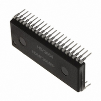
M38513E4FP#U0 Renesas Electronics America, M38513E4FP#U0 Datasheet - Page 56

M38513E4FP#U0
Manufacturer Part Number
M38513E4FP#U0
Description
IC 740 MCU ROM 16K 42SSOP
Manufacturer
Renesas Electronics America
Series
740/38000r
Specifications of M38513E4FP#U0
Core Processor
740
Core Size
8-Bit
Speed
8MHz
Connectivity
SIO, UART/USART
Peripherals
PWM, WDT
Number Of I /o
34
Program Memory Size
16KB (16K x 8)
Program Memory Type
OTP
Ram Size
512 x 8
Voltage - Supply (vcc/vdd)
2.7 V ~ 5.5 V
Data Converters
A/D 5x10b
Oscillator Type
External
Operating Temperature
-20°C ~ 85°C
Package / Case
42-SSOP
Package
42SSOP
Family Name
740
Maximum Speed
8 MHz
Operating Supply Voltage
5 V
Data Bus Width
8 Bit
Number Of Programmable I/os
34
Interface Type
I2C-BUS
On-chip Adc
5-chx10-bit
Number Of Timers
4
Lead Free Status / RoHS Status
Contains lead / RoHS non-compliant
Eeprom Size
-
3851 Group
Software Commands (CPU Rewrite Mode)
Table 16 lists the software commands.
After setting the CPU Rewrite Mode Select Bit of the flash memory
control register to “1”, execute a software command to specify an
erase or program operation.
Each software command is explained below.
The read array mode is entered by writing the command code
“FF
one of the bus cycles that follow, the contents of the specified ad-
dress are read out at the data bus (D
The read array mode is retained intact until another command is
written.
The read status register mode is entered by writing the command
code “70
ter are read out at the data bus (D
bus cycle.
The status register is explained in the next section.
This command is used to clear the bits SR1, SR4, and SR5 of the
status register after they have been set. These bits indicate that
operation has ended in an error. To use this command, write the
command code “50
Program operation starts when the command code “40
ten in the first bus cycle. Then, if the address and data to program
are written in the 2nd bus cycle, program operation (data program-
ming and verification) will start.
Whether the write operation is completed can be confirmed by
reading the status register or the RY/BY Status Flag of the flash
memory control register. When the program starts, the read status
Table 16 List of software commands (CPU rewrite mode)
Rev.1.01
Notes 1: X denotes a given address in the User ROM area .
Read Array Command (FF
Read Status Register Command (70
Clear Status Register Command (50
Program Command (40
R e a d a r r a y
R e a d s t a t u s r e g i s t e r
C l e a r s t a t u s r e g i s t e r
P r o g r a m
E r a s e a l l b l o c k s
B l o c k e r a s e
16
” in the first bus cycle. When an address to be read is input in
2: SRD = Status Register Data
3: WA = Write Address, WD = Write Data
4: BA = Block Address to be erased (Input the maximum address of each block.)
16
” in the first bus cycle. The contents of the status regis-
Oct 15, 2003
Command
(Built-in 24 KB or more ROM)
16
” in the first bus cycle.
16
)
16
page 54 of 89
)
0
to D
0
_____
to D
16
7
16
) by a read in the second
C y c l e n u m b e r
)
)
7
).
1
2
1
2
2
2
16
” is writ-
Mode
W r i t e
W r i t e
W r i t e
W r i t e
W r i t e
W r i t e
Address
register mode is entered automatically and the contents of the sta-
tus register is read at the data bus (D
bit 7 (SR7) is set to “0” at the same time the write operation starts
and is returned to “1” upon completion of the write operation. In
this case, the read status register mode remains active until the
next command is written.
The RY/BY Status Flag is “0” (busy) during write operation and “1”
(ready) when the write operation is completed as is the status reg-
ister bit 7.
At program end, program results can be checked by reading bit 4
(SR4) of the status register.
Fig. 60 Program flowchart
X
First bus cycle
(Note 1)
X
X
X
X
X
Write
(Read array command
____
Program completed
( D
S t a t u s r e g i s t e r
“FF
Write 40
S R 4 = 0 ?
D a t a
0
W r i t e a d d r e s s
W r i t e d a t a
R Y / B Y = 1 ?
S R 7 = 1 ?
t o D
F F
7 0
4 0
2 0
2 0
5 0
S t a r t
r e a d
16
1 6
1 6
1 6
1 6
1 6
1 6
o r
” write)
7
)
Y E S
Y E S
16
Mode
R e a d
W r i t e
W r i t e
W r i t e
NO
NO
S e c o n d b u s c y c l e
W A
B A
0
A d d r e s s
to D
X
(Note 4)
X
(Note 3)
7
). The status register
P r o g r a m
e r r o r
S R D
W D
(D
0
Data
2 0
D 0
to D
(Note 2)
( N o t e 3 )
1 6
1 6
7
)


