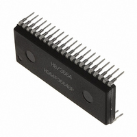
M38513E4FP#U0 Renesas Electronics America, M38513E4FP#U0 Datasheet - Page 24

M38513E4FP#U0
Manufacturer Part Number
M38513E4FP#U0
Description
IC 740 MCU ROM 16K 42SSOP
Manufacturer
Renesas Electronics America
Series
740/38000r
Specifications of M38513E4FP#U0
Core Processor
740
Core Size
8-Bit
Speed
8MHz
Connectivity
SIO, UART/USART
Peripherals
PWM, WDT
Number Of I /o
34
Program Memory Size
16KB (16K x 8)
Program Memory Type
OTP
Ram Size
512 x 8
Voltage - Supply (vcc/vdd)
2.7 V ~ 5.5 V
Data Converters
A/D 5x10b
Oscillator Type
External
Operating Temperature
-20°C ~ 85°C
Package / Case
42-SSOP
Package
42SSOP
Family Name
740
Maximum Speed
8 MHz
Operating Supply Voltage
5 V
Data Bus Width
8 Bit
Number Of Programmable I/os
34
Interface Type
I2C-BUS
On-chip Adc
5-chx10-bit
Number Of Timers
4
Lead Free Status / RoHS Status
Contains lead / RoHS non-compliant
Eeprom Size
-
3851 Group
SERIAL I/O
Serial I/O1 can be used as either clock synchronous or asynchro-
nous (UART) serial I/O. A dedicated timer is also provided for
baud rate generation.
Fig. 18 Block diagram of clock synchronous serial I/O1
Fig. 19 Operation of clock synchronous serial I/O1 function
Rev.1.01
SERIAL I/O1
Write pulse to receive/transmit
buffer register (address 0018
Receive enable signal S
Transfer shift clock
(1/2 to 1/2048 of the internal
clock, or an external clock)
P2
Notes 1: As the transmit interrupt (TI), either when the transmit buffer has emptied (TBE=1) or after the transmit shift operation has
7
/CNTR
Oct 15, 2003
P2
(Built-in 24 KB or more ROM)
P2
P2
2: If data is written to the transmit buffer register when TSC=0, the transmit clock is generated continuously and serial data
3: The receive interrupt (RI) is set when the receive buffer full flag (RBF) becomes “1” .
Serial output TxD
0
6
Serial input RxD
/S
/S
4
5
ended (TSC=1), by setting the transmit interrupt source selection bit (TIC) of the serial I/O1 control register.
is output continuously from the TxD pin.
/R
/T
RDY1
CLK1
X
X
X
IN
D
D
RDY1
BRG count source selection bit
page 22 of 89
16
F/F
)
TBE = 0
1/4
Falling-edge detector
TBE = 1
TSC = 0
D
D
Receive buffer register
0
0
Receive shift register
Transmit buffer register
Transmit shift register
Data bus
Data bus
D
D
1
1
Address 0018
Shift clock
Serial I/O1 synchronous
clock selection bit
Frequency division ratio 1/(n+1)
Baud rate generator
Address 0018
Shift clock
Address 001C
D
D
2
2
(1) Clock Synchronous Serial I/O Mode
Clock synchronous serial I/O mode can be selected by setting the
serial I/O1 mode selection bit of the serial I/O1 control register (bit
6 of address 001A
For clock synchronous serial I/O, the transmitter and the receiver
must use the same clock. If an internal clock is used, transfer is
started by a write signal to the TB/RB.
16
16
Clock control circuit
Clock control circuit
D
D
16
3
3
Serial I/O1 control register
Transmit interrupt source selection bit
Receive buffer full flag (RBF)
Serial I/O1 status register
1/4
D
D
16
4
4
) to “1”.
Receive interrupt request (RI)
D
D
Transmit buffer empty flag (TBE)
Transmit shift completion flag (TSC)
5
5
Transmit interrupt request (TI)
Address 001A
D
D
Address 0019
6
6
Overrun error (OE)
detection
RBF = 1
TSC = 1
D
D
16
7
7
16


