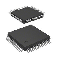
DF36054GFPJ Renesas Electronics America, DF36054GFPJ Datasheet - Page 123

DF36054GFPJ
Manufacturer Part Number
DF36054GFPJ
Description
MCU 3/5V 32K J-TEMP POR&LVD 64-Q
Manufacturer
Renesas Electronics America
Series
H8® H8/300H Tinyr
Datasheet
1.DF36057GFZV.pdf
(594 pages)
Specifications of DF36054GFPJ
Core Processor
H8/300H
Core Size
16-Bit
Speed
20MHz
Connectivity
CAN, SCI, SSU
Peripherals
LVD, POR, PWM, WDT
Number Of I /o
45
Program Memory Size
32KB (32K x 8)
Program Memory Type
FLASH
Ram Size
2K x 8
Voltage - Supply (vcc/vdd)
3 V ~ 5.5 V
Data Converters
A/D 8x10b
Oscillator Type
Internal
Operating Temperature
-40°C ~ 85°C
Package / Case
64-LQFP
Lead Free Status / RoHS Status
Contains lead / RoHS non-compliant
Eeprom Size
-
Other names
HD64F36054GFPJ
HD64F36054GFPJ
HD64F36054GFPJ
- Current page: 123 of 594
- Download datasheet (4Mb)
The features of the 56-kbyte or 32-kbyte flash memories built into the flash memory (F-ZTAT)
version are summarized below.
7.1
Figure 7.1 shows the block configuration of flash memory. The thick lines indicate erasing units,
the narrow lines indicate programming units, and the values are addresses. The 56-kbyte flash
memory is divided into 1 kbyte 4 blocks, 28 kbytes 1 block, 16 kbytes 1 block, and 8 kbytes
Erasing is performed in these units. Programming is performed in 128-byte units starting from an
address with lower eight bits H'00 or H'80.
1 block. The 32-kbyte flash memory is divided into 1 kbyte 4 blocks and 28 kbytes 1 blocks.
Programming/erase methods
Reprogramming capability
On-board programming
Programmer mode
Automatic bit rate adjustment
Programming/erasing protection
Power-down mode
The flash memory is programmed 128 bytes at a time. Erase is performed in single-block
units. The flash memory is configured as follows: 1 kbyte 4 blocks, 28 kbytes 1 block,
16 kbytes 1 block, and 8 kbytes 1 block for the H8/36057F and H8/36037F and 1 kbyte
flash memory, each block must be erased in turn.
The flash memory can be reprogrammed up to 1,000 times.
On-board programming/erasing can be done in boot mode, in which the boot program built
into the chip is started to erase or program of the entire flash memory. In normal user
program mode, individual blocks can be erased or programmed.
Flash memory can be programmed/erased in programmer mode using a PROM
programmer, as well as in on-board programming mode.
For data transfer in boot mode, this LSI's bit rate can be automatically adjusted to match
the transfer bit rate of the host.
Sets software protection against flash memory programming/erasing.
Operation of the power supply circuit can be partly halted in subactive mode. As a result,
flash memory can be read with low power consumption.
4 blocks and 28 kbytes
Block Configuration
1 block for the H8/36054F and H8/36034F. To erase the entire
Section 7 ROM
Rev. 4.00 Mar. 15, 2006 Page 89 of 556
REJ09B0026-0400
Section 7 ROM
Related parts for DF36054GFPJ
Image
Part Number
Description
Manufacturer
Datasheet
Request
R

Part Number:
Description:
Headers & Wire Housings 20P PLUG METAL COVER
Manufacturer:
Hirose Electric Co Ltd

Part Number:
Description:
Headers & Wire Housings 25P PLUG METAL COVER
Manufacturer:
Hirose Electric Co Ltd

Part Number:
Description:
Headers & Wire Housings 15P PLUG METAL COVER
Manufacturer:
Hirose Electric Co Ltd

Part Number:
Description:
0.4 Mm Pitch, 1.5 Mm Mated Height, Board-to-fine Coaxial Cable Connectors
Manufacturer:
Hirose Electric
Datasheet:

Part Number:
Description:
CONN RECEPT 40POS 0.4MM SMD GOLD
Manufacturer:
Hirose Electric Co Ltd
Datasheet:

Part Number:
Description:
KIT STARTER FOR M16C/29
Manufacturer:
Renesas Electronics America
Datasheet:

Part Number:
Description:
KIT STARTER FOR R8C/2D
Manufacturer:
Renesas Electronics America
Datasheet:

Part Number:
Description:
R0K33062P STARTER KIT
Manufacturer:
Renesas Electronics America
Datasheet:

Part Number:
Description:
KIT STARTER FOR R8C/23 E8A
Manufacturer:
Renesas Electronics America
Datasheet:

Part Number:
Description:
KIT STARTER FOR R8C/25
Manufacturer:
Renesas Electronics America
Datasheet:

Part Number:
Description:
KIT STARTER H8S2456 SHARPE DSPLY
Manufacturer:
Renesas Electronics America
Datasheet:

Part Number:
Description:
KIT STARTER FOR R8C38C
Manufacturer:
Renesas Electronics America
Datasheet:

Part Number:
Description:
KIT STARTER FOR R8C35C
Manufacturer:
Renesas Electronics America
Datasheet:

Part Number:
Description:
KIT STARTER FOR R8CL3AC+LCD APPS
Manufacturer:
Renesas Electronics America
Datasheet:

Part Number:
Description:
KIT STARTER FOR RX610
Manufacturer:
Renesas Electronics America
Datasheet:


