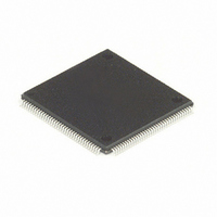
MC68HC16Z1CAG25 Freescale Semiconductor, MC68HC16Z1CAG25 Datasheet - Page 419

MC68HC16Z1CAG25
Manufacturer Part Number
MC68HC16Z1CAG25
Description
IC MCU 16BIT 25MHZ 144-LQFP
Manufacturer
Freescale Semiconductor
Series
HC16r
Datasheet
1.MC68HC16Z1VEH16.pdf
(500 pages)
Specifications of MC68HC16Z1CAG25
Core Processor
CPU16
Core Size
16-Bit
Speed
25MHz
Connectivity
EBI/EMI, SCI, SPI
Peripherals
POR, PWM, WDT
Number Of I /o
16
Program Memory Type
ROMless
Ram Size
1K x 8
Voltage - Supply (vcc/vdd)
2.7 V ~ 5.5 V
Data Converters
A/D 8x10b
Oscillator Type
Internal
Operating Temperature
-40°C ~ 85°C
Package / Case
144-LQFP
Cpu Family
HC16
Device Core Size
16b
Frequency (max)
25MHz
Interface Type
SCI/SPI/UART
Program Memory Size
Not Required
Total Internal Ram Size
1KB
# I/os (max)
16
Number Of Timers - General Purpose
11
Operating Supply Voltage (typ)
3.3/5V
Operating Supply Voltage (max)
5.5V
Operating Supply Voltage (min)
2.7V
On-chip Adc
8-chx10-bit
Instruction Set Architecture
CISC
Operating Temp Range
-40C to 85C
Operating Temperature Classification
Industrial
Mounting
Surface Mount
Pin Count
144
Package Type
LQFP
Controller Family/series
68HC16
No. Of I/o's
16
Ram Memory Size
1KB
Cpu Speed
25MHz
No. Of Timers
2
Embedded Interface Type
QSPI, SCI
Rohs Compliant
Yes
Processor Series
HC16Z
Core
CPU16
Data Bus Width
16 bit
Data Ram Size
1 KB
Maximum Clock Frequency
25 MHz
Number Of Programmable I/os
16
Number Of Timers
11
Maximum Operating Temperature
+ 85 C
Mounting Style
SMD/SMT
Minimum Operating Temperature
- 40 C
Lead Free Status / RoHS Status
Lead free / RoHS Compliant
Eeprom Size
-
Program Memory Size
-
Lead Free Status / Rohs Status
Compliant
Available stocks
Company
Part Number
Manufacturer
Quantity
Price
Company:
Part Number:
MC68HC16Z1CAG25
Manufacturer:
FREESCAL
Quantity:
455
Company:
Part Number:
MC68HC16Z1CAG25
Manufacturer:
Freescale Semiconductor
Quantity:
10 000
- Current page: 419 of 500
- Download datasheet (6Mb)
PQSPAR — PORT QS Pin Assignment Register
DDRQS — PORT QS Data Direction Register
USED
D.6.9 Port QS Pin Assignment Register/Data Direction Register
M68HC16 Z SERIES
USER’S MANUAL
NOT
15
RESET:
Clearing a bit in PQSPAR assigns the corresponding pin to general-purpose I/O. Set-
ting a bit assigns the pin to the QSPI. PQSPAR does not affect operation of the SCI.
Table D-33
DDRQS determines whether pins configured for general-purpose I/O are inputs or out-
puts. Clearing a bit makes the corresponding pin an input; setting a bit makes the pin
an output. DDRQS affects both QSPI function and I/O
effect of DDRQS on QSM pin function.
PQSPA6 PQSPA5 PQSPA4 PQSPA3
14
0
13
0
displays PQSPAR pin assignments.
NOTES:
12
0
1. PQS2 is a digital I/O pin unless the SPI is enabled (SPE set in
2. PQS7 is a digital I/O pin unless the SCI transmitter is enabled (TE set
PQSPAR Field
SPCR1), in which case it becomes the QSPI serial clock SCK.
in SCCR1), in which case it becomes the SCI serial output TXD.
PQSPA0
PQSPA1
PQSPA3
PQSPA4
PQSPA5
PQSPA6
Freescale Semiconductor, Inc.
Table D-33 PQSPAR Pin Assignments
11
—
—
0
For More Information On This Product,
USED
NOT
10
Go to: www.freescale.com
PQSPA1 PQSPA0 DDQS7 DDQS6 DDQS5 DDQS4 DDQS3 DDQS2 DDQS1 DDQS0
REGISTER SUMMARY
9
0
PQSPAR Bit
8
0
—
—
—
—
0
1
0
1
0
1
0
1
0
1
0
1
7
0
6
0
function.Table D-34
Pin Function
5
0
PCS0/SS
PQS2
PQS7
PQS0
MISO
PQS1
MOSI
PQS3
PQS4
PCS1
PQS5
PCS2
PQS6
PCS3
SCK
TXD
4
0
1
2
3
0
2
0
$YFFC16
$YFFC17
shows the
1
0
D-45
0
0
Related parts for MC68HC16Z1CAG25
Image
Part Number
Description
Manufacturer
Datasheet
Request
R
Part Number:
Description:
Manufacturer:
Freescale Semiconductor, Inc
Datasheet:
Part Number:
Description:
Manufacturer:
Freescale Semiconductor, Inc
Datasheet:
Part Number:
Description:
Manufacturer:
Freescale Semiconductor, Inc
Datasheet:
Part Number:
Description:
Manufacturer:
Freescale Semiconductor, Inc
Datasheet:
Part Number:
Description:
Manufacturer:
Freescale Semiconductor, Inc
Datasheet:
Part Number:
Description:
Manufacturer:
Freescale Semiconductor, Inc
Datasheet:
Part Number:
Description:
Manufacturer:
Freescale Semiconductor, Inc
Datasheet:
Part Number:
Description:
Manufacturer:
Freescale Semiconductor, Inc
Datasheet:
Part Number:
Description:
Manufacturer:
Freescale Semiconductor, Inc
Datasheet:
Part Number:
Description:
Manufacturer:
Freescale Semiconductor, Inc
Datasheet:
Part Number:
Description:
Manufacturer:
Freescale Semiconductor, Inc
Datasheet:
Part Number:
Description:
Manufacturer:
Freescale Semiconductor, Inc
Datasheet:
Part Number:
Description:
Manufacturer:
Freescale Semiconductor, Inc
Datasheet:
Part Number:
Description:
Manufacturer:
Freescale Semiconductor, Inc
Datasheet:
Part Number:
Description:
Manufacturer:
Freescale Semiconductor, Inc
Datasheet:


