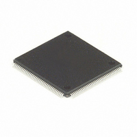
MC68HC16Z1CAG25 Freescale Semiconductor, MC68HC16Z1CAG25 Datasheet - Page 242

MC68HC16Z1CAG25
Manufacturer Part Number
MC68HC16Z1CAG25
Description
IC MCU 16BIT 25MHZ 144-LQFP
Manufacturer
Freescale Semiconductor
Series
HC16r
Datasheet
1.MC68HC16Z1VEH16.pdf
(500 pages)
Specifications of MC68HC16Z1CAG25
Core Processor
CPU16
Core Size
16-Bit
Speed
25MHz
Connectivity
EBI/EMI, SCI, SPI
Peripherals
POR, PWM, WDT
Number Of I /o
16
Program Memory Type
ROMless
Ram Size
1K x 8
Voltage - Supply (vcc/vdd)
2.7 V ~ 5.5 V
Data Converters
A/D 8x10b
Oscillator Type
Internal
Operating Temperature
-40°C ~ 85°C
Package / Case
144-LQFP
Cpu Family
HC16
Device Core Size
16b
Frequency (max)
25MHz
Interface Type
SCI/SPI/UART
Program Memory Size
Not Required
Total Internal Ram Size
1KB
# I/os (max)
16
Number Of Timers - General Purpose
11
Operating Supply Voltage (typ)
3.3/5V
Operating Supply Voltage (max)
5.5V
Operating Supply Voltage (min)
2.7V
On-chip Adc
8-chx10-bit
Instruction Set Architecture
CISC
Operating Temp Range
-40C to 85C
Operating Temperature Classification
Industrial
Mounting
Surface Mount
Pin Count
144
Package Type
LQFP
Controller Family/series
68HC16
No. Of I/o's
16
Ram Memory Size
1KB
Cpu Speed
25MHz
No. Of Timers
2
Embedded Interface Type
QSPI, SCI
Rohs Compliant
Yes
Processor Series
HC16Z
Core
CPU16
Data Bus Width
16 bit
Data Ram Size
1 KB
Maximum Clock Frequency
25 MHz
Number Of Programmable I/os
16
Number Of Timers
11
Maximum Operating Temperature
+ 85 C
Mounting Style
SMD/SMT
Minimum Operating Temperature
- 40 C
Lead Free Status / RoHS Status
Lead free / RoHS Compliant
Eeprom Size
-
Program Memory Size
-
Lead Free Status / Rohs Status
Compliant
Available stocks
Company
Part Number
Manufacturer
Quantity
Price
Company:
Part Number:
MC68HC16Z1CAG25
Manufacturer:
FREESCAL
Quantity:
455
Company:
Part Number:
MC68HC16Z1CAG25
Manufacturer:
Freescale Semiconductor
Quantity:
10 000
- Current page: 242 of 500
- Download datasheet (6Mb)
10.2 MCCI Registers and Address Map
10.2.1 MCCI Global Registers
10.2.1.1 Low-Power Stop Mode
10-2
The SCI is a universal asynchronous receiver transmitter (UART) serial interface with
a standard non-return to zero (NRZ) mark/space format. It operates in either full- or
half-duplex mode. It also contains separate transmit and receive enable bits and a
double-transmit buffer. A modulus-type baud rate generator provides rates from 64
baud to 524 kbaud with a 16.78-MHz system clock. Word length of either eight or nine
bits is software selectable. Optional parity generation and detection provide either
even or odd parity check capability. Advanced error detection circuitry catches glitches
of up to 1/16 of a bit time in duration. Wakeup functions allow the CPU to run uninter-
rupted until meaningful data is received.
The MCCI address map occupies 64 bytes from address $YFFC00 to $YFFC3F. It
consists of MCCI global registers and SPI and SCI control, status, and data registers.
Writes to unimplemented register bits have no effect, and reads of unimplemented bits
always return zero.
The MM bit in the system integration module configuration register (SIMCR) defines
the most significant bit (ADDR23) of the IMB address for each module. Because
ADDR[23:20] are driven to the same bit as ADDR19, MM must be set to one. If MM is
cleared, IMB modules are inaccessible. Refer to
formation about how the state of MM affects the system.
The MCCI module configuration register (MMCR) contains bits and fields to place the
MCCI in low-power operation, establish the privilege level required to access MCCI
registers, and establish the priority of the MCCI during interrupt arbitration. The MCCI
test register (MTEST) is used only during factory test of the MCCI. The SCI interrupt
level register (ILSCI) determines the level of interrupts requested by each SCI. Sepa-
rate fields hold the interrupt-request levels for SCIA and SCIB. The MCCI interrupt
vector register (MIVR) determines which three vectors in the exception vector table
are to be used for MCCI interrupts. The SPI and both SCI interfaces have separate
interrupt vectors adjacent to one another. The SPI interrupt level register (ILSPI) de-
termines the priority level of interrupts requested by the SPI. The MCCI port data reg-
isters (PORTMC and PORTMCP) are used to configure port MCCI for general-
purpose I/O. The MCCI pin assignment register (MPAR) determines which of the SPI
pins (with the exception of SCK) are used by the SPI, and which pins are available for
general-purpose I/O. The MCCI data direction register (MDDR) configures each pin as
an input or output.
When the STOP bit in the MMCR is set, the IMB clock signal to most of the MCCI mod-
ule is disabled. This places the module in an idle state and minimizes power consump-
tion.
MULTICHANNEL COMMUNICATION INTERFACE
Freescale Semiconductor, Inc.
For More Information On This Product,
Go to: www.freescale.com
5.2.1 Module Mapping
M68HC16 Z SERIES
USER’S MANUAL
for more in-
Related parts for MC68HC16Z1CAG25
Image
Part Number
Description
Manufacturer
Datasheet
Request
R
Part Number:
Description:
Manufacturer:
Freescale Semiconductor, Inc
Datasheet:
Part Number:
Description:
Manufacturer:
Freescale Semiconductor, Inc
Datasheet:
Part Number:
Description:
Manufacturer:
Freescale Semiconductor, Inc
Datasheet:
Part Number:
Description:
Manufacturer:
Freescale Semiconductor, Inc
Datasheet:
Part Number:
Description:
Manufacturer:
Freescale Semiconductor, Inc
Datasheet:
Part Number:
Description:
Manufacturer:
Freescale Semiconductor, Inc
Datasheet:
Part Number:
Description:
Manufacturer:
Freescale Semiconductor, Inc
Datasheet:
Part Number:
Description:
Manufacturer:
Freescale Semiconductor, Inc
Datasheet:
Part Number:
Description:
Manufacturer:
Freescale Semiconductor, Inc
Datasheet:
Part Number:
Description:
Manufacturer:
Freescale Semiconductor, Inc
Datasheet:
Part Number:
Description:
Manufacturer:
Freescale Semiconductor, Inc
Datasheet:
Part Number:
Description:
Manufacturer:
Freescale Semiconductor, Inc
Datasheet:
Part Number:
Description:
Manufacturer:
Freescale Semiconductor, Inc
Datasheet:
Part Number:
Description:
Manufacturer:
Freescale Semiconductor, Inc
Datasheet:
Part Number:
Description:
Manufacturer:
Freescale Semiconductor, Inc
Datasheet:


