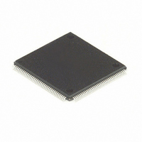
MC68HC16Z1CAG25 Freescale Semiconductor, MC68HC16Z1CAG25 Datasheet - Page 162

MC68HC16Z1CAG25
Manufacturer Part Number
MC68HC16Z1CAG25
Description
IC MCU 16BIT 25MHZ 144-LQFP
Manufacturer
Freescale Semiconductor
Series
HC16r
Datasheet
1.MC68HC16Z1VEH16.pdf
(500 pages)
Specifications of MC68HC16Z1CAG25
Core Processor
CPU16
Core Size
16-Bit
Speed
25MHz
Connectivity
EBI/EMI, SCI, SPI
Peripherals
POR, PWM, WDT
Number Of I /o
16
Program Memory Type
ROMless
Ram Size
1K x 8
Voltage - Supply (vcc/vdd)
2.7 V ~ 5.5 V
Data Converters
A/D 8x10b
Oscillator Type
Internal
Operating Temperature
-40°C ~ 85°C
Package / Case
144-LQFP
Cpu Family
HC16
Device Core Size
16b
Frequency (max)
25MHz
Interface Type
SCI/SPI/UART
Program Memory Size
Not Required
Total Internal Ram Size
1KB
# I/os (max)
16
Number Of Timers - General Purpose
11
Operating Supply Voltage (typ)
3.3/5V
Operating Supply Voltage (max)
5.5V
Operating Supply Voltage (min)
2.7V
On-chip Adc
8-chx10-bit
Instruction Set Architecture
CISC
Operating Temp Range
-40C to 85C
Operating Temperature Classification
Industrial
Mounting
Surface Mount
Pin Count
144
Package Type
LQFP
Controller Family/series
68HC16
No. Of I/o's
16
Ram Memory Size
1KB
Cpu Speed
25MHz
No. Of Timers
2
Embedded Interface Type
QSPI, SCI
Rohs Compliant
Yes
Processor Series
HC16Z
Core
CPU16
Data Bus Width
16 bit
Data Ram Size
1 KB
Maximum Clock Frequency
25 MHz
Number Of Programmable I/os
16
Number Of Timers
11
Maximum Operating Temperature
+ 85 C
Mounting Style
SMD/SMT
Minimum Operating Temperature
- 40 C
Lead Free Status / RoHS Status
Lead free / RoHS Compliant
Eeprom Size
-
Program Memory Size
-
Lead Free Status / Rohs Status
Compliant
Available stocks
Company
Part Number
Manufacturer
Quantity
Price
Company:
Part Number:
MC68HC16Z1CAG25
Manufacturer:
FREESCAL
Quantity:
455
Company:
Part Number:
MC68HC16Z1CAG25
Manufacturer:
Freescale Semiconductor
Quantity:
10 000
- Current page: 162 of 500
- Download datasheet (6Mb)
5.7.8 Use of the Three-State Control Pin
5-56
CLKOUT
CYCLES
RESET
NOTES:
V
LOCK
VCO
BUS
1. INTERNAL START-UP TIME
2. FIRST INSTRUCTION FETCHED
DD
The SIM clock synthesizer provides clock signals to the other MCU modules. After the
clock is running and MSTRST is asserted for at least four clock cycles, these modules
reset. V
cles take. Worst case is approximately 15 milliseconds. During this period, module
port pins may be in an indeterminate state. While input-only pins can be put in a known
state by external pull-up resistors, external logic on input/output or output-only pins
during this time must condition the lines. Active drivers require high-impedance buffers
or isolation resistors to prevent conflict.
Figure 5-20
RESET, V
Asserting the three-state control (TSC) input causes the MCU to put all output drivers
in a disabled, high-impedance state. The signal must remain asserted for approxi-
mately ten clock cycles in order for drivers to change state.
When the internal clock synthesizer is used (MODCLK held high during reset), synthe-
sizer ramp-up time affects how long the ten cycles take. Worst case is approximately
20 milliseconds from TSC assertion.
When an external clock signal is applied (MODCLK held low during reset), pins go to
high-impedance state as soon after TSC assertion as approximately ten clock pulses
have been applied to the EXTAL pin.
BUS STATE
UNKNOWN
DD
DD
ramp time and VCO frequency ramp time determine how long the four cy-
is a timing diagram for power-on reset. It shows the relationships between
, and bus signals.
2 CLOCKS
Freescale Semiconductor, Inc.
CONTROL SIGNALS
For More Information On This Product,
THREE-STATED
ADDRESS AND
Figure 5-20 Power-On Reset
SYSTEM INTEGRATION MODULE
512 CLOCKS
Go to: www.freescale.com
10 CLOCKS
1
M68HC16 Z SERIES
USER’S MANUAL
2
16 POR TIM
Related parts for MC68HC16Z1CAG25
Image
Part Number
Description
Manufacturer
Datasheet
Request
R
Part Number:
Description:
Manufacturer:
Freescale Semiconductor, Inc
Datasheet:
Part Number:
Description:
Manufacturer:
Freescale Semiconductor, Inc
Datasheet:
Part Number:
Description:
Manufacturer:
Freescale Semiconductor, Inc
Datasheet:
Part Number:
Description:
Manufacturer:
Freescale Semiconductor, Inc
Datasheet:
Part Number:
Description:
Manufacturer:
Freescale Semiconductor, Inc
Datasheet:
Part Number:
Description:
Manufacturer:
Freescale Semiconductor, Inc
Datasheet:
Part Number:
Description:
Manufacturer:
Freescale Semiconductor, Inc
Datasheet:
Part Number:
Description:
Manufacturer:
Freescale Semiconductor, Inc
Datasheet:
Part Number:
Description:
Manufacturer:
Freescale Semiconductor, Inc
Datasheet:
Part Number:
Description:
Manufacturer:
Freescale Semiconductor, Inc
Datasheet:
Part Number:
Description:
Manufacturer:
Freescale Semiconductor, Inc
Datasheet:
Part Number:
Description:
Manufacturer:
Freescale Semiconductor, Inc
Datasheet:
Part Number:
Description:
Manufacturer:
Freescale Semiconductor, Inc
Datasheet:
Part Number:
Description:
Manufacturer:
Freescale Semiconductor, Inc
Datasheet:
Part Number:
Description:
Manufacturer:
Freescale Semiconductor, Inc
Datasheet:


