C8051F521A-IM Silicon Laboratories Inc, C8051F521A-IM Datasheet - Page 9
C8051F521A-IM
Manufacturer Part Number
C8051F521A-IM
Description
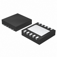
IC 8051 MCU 8K FLASH 10DFN
Manufacturer
Silicon Laboratories Inc
Series
C8051F52xr
Specifications of C8051F521A-IM
Program Memory Type
FLASH
Program Memory Size
8KB (8K x 8)
Package / Case
10-DFN
Core Processor
8051
Core Size
8-Bit
Speed
25MHz
Connectivity
SPI, UART/USART
Peripherals
Brown-out Detect/Reset, POR, PWM, Temp Sensor, WDT
Number Of I /o
6
Ram Size
256 x 8
Voltage - Supply (vcc/vdd)
1.8 V ~ 5.25 V
Data Converters
A/D 6x12b
Oscillator Type
Internal
Operating Temperature
-40°C ~ 125°C
Processor Series
C8051F5x
Core
8051
Data Bus Width
8 bit
Data Ram Size
256 B
Interface Type
SPI/UART
Maximum Clock Frequency
25 MHz
Number Of Programmable I/os
6
Number Of Timers
3
Maximum Operating Temperature
+ 125 C
Mounting Style
SMD/SMT
3rd Party Development Tools
PK51, CA51, A51, ULINK2
Development Tools By Supplier
C8051F500DK
Minimum Operating Temperature
- 40 C
On-chip Adc
6-ch x 12-bit
Lead Free Status / RoHS Status
Lead free / RoHS Compliant
For Use With
336-1488 - KIT DEV C8051F53XA, C8051F52XA770-1006 - ISP 4PORT FOR SILABS C8051F MCU336-1455 - ADAPTER PROGRAM TOOLSTICK F520
Eeprom Size
-
Lead Free Status / Rohs Status
Lead free / RoHS Compliant
Other names
336-1490-5


C8051F52x/F52xA/F53x/F53xA
List of Tables
Table 1.1. Product Selection Guide (Recommended for New Designs) .................. 14
Table 1.2. Product Selection Guide (Not Recommended for New Designs) ........... 15
Table 1.3. Operating Modes Summary .................................................................... 21
Table 2.1. Absolute Maximum Ratings .................................................................... 25
Table 2.2. Global DC Electrical Characteristics ....................................................... 26
Table 2.3. ADC0 Electrical Characteristics .............................................................. 29
Table 2.4. Voltage Reference Electrical Characteristics ......................................... 30
Table 2.5. Voltage Regulator Electrical Specifications ............................................ 30
Table 2.6. Comparator Electrical Characteristics .................................................... 31
Table 2.7. Reset Electrical Characteristics .............................................................. 32
Table 2.8. Flash Electrical Characteristics .............................................................. 33
Table 2.9. Port I/O DC Electrical Characteristics ..................................................... 33
Table 2.10. Oscillator Electrical Characteristics ...................................................... 34
Table 3.1. Pin Definitions for the C8051F52x and C8051F52xA (DFN 10) ............. 36
Table 3.2. DFN-10 Package Diagram Dimensions .................................................. 38
Table 3.3. DFN-10 Landing Diagram Dimensions ................................................... 39
Table 3.4. Pin Definitions for the C8051F53x and C805153xA (TSSOP 20) .......... 40
Table 3.5. TSSOP-20 Package Diagram Dimensions ............................................. 43
Table 3.6. TSSOP-20 Landing Diagram Dimensions .............................................. 44
Table 3.7. Pin Definitions for the C8051F53x and C805153xA (QFN 20) ............... 46
Table 3.8. QFN-20 Package Diagram Dimensions ................................................. 49
Table 3.9. QFN-20 Landing Diagram Dimensions ................................................... 51
Table 8.1. CIP-51 Instruction Set Summary ............................................................ 83
Table 9.1. Special Function Register (SFR) Memory Map ...................................... 94
Table 9.2. Special Function Registers ..................................................................... 95
Table 10.1. Interrupt Summary ................................................................................ 99
Table 12.1. Flash Security Summary .................................................................... 117
Table 15.1. Timer Settings for Standard Baud Rates
Using the Internal Oscillator ............................................................... 149
Table 16.1. SPI Slave Timing Parameters ............................................................ 162
Table 17.1. Baud-Rate Calculation Variable Ranges ............................................ 165
Table 17.2. Manual Baud Rate Parameters Examples ......................................... 166
Table 17.3. Autobaud Parameters Examples ........................................................ 167
Table 17.4. LIN Registers* (Indirectly Addressable) .............................................. 173
Table 19.1. PCA Timebase Input Options ............................................................. 195
Table 19.2. PCA0CPM Register Settings for PCA Capture/Compare Modules .... 196
Table 19.3. Watchdog Timer Timeout Intervals1 ................................................... 204
Rev. 1.3
9
Related parts for C8051F521A-IM
Image
Part Number
Description
Manufacturer
Datasheet
Request
R

Part Number:
Description:
SMD/C°/SINGLE-ENDED OUTPUT SILICON OSCILLATOR
Manufacturer:
Silicon Laboratories Inc
Part Number:
Description:
Manufacturer:
Silicon Laboratories Inc
Datasheet:
Part Number:
Description:
N/A N/A/SI4010 AES KEYFOB DEMO WITH LCD RX
Manufacturer:
Silicon Laboratories Inc
Datasheet:
Part Number:
Description:
N/A N/A/SI4010 SIMPLIFIED KEY FOB DEMO WITH LED RX
Manufacturer:
Silicon Laboratories Inc
Datasheet:
Part Number:
Description:
N/A/-40 TO 85 OC/EZLINK MODULE; F930/4432 HIGH BAND (REV E/B1)
Manufacturer:
Silicon Laboratories Inc
Part Number:
Description:
EZLink Module; F930/4432 Low Band (rev e/B1)
Manufacturer:
Silicon Laboratories Inc
Part Number:
Description:
I°/4460 10 DBM RADIO TEST CARD 434 MHZ
Manufacturer:
Silicon Laboratories Inc
Part Number:
Description:
I°/4461 14 DBM RADIO TEST CARD 868 MHZ
Manufacturer:
Silicon Laboratories Inc
Part Number:
Description:
I°/4463 20 DBM RFSWITCH RADIO TEST CARD 460 MHZ
Manufacturer:
Silicon Laboratories Inc
Part Number:
Description:
I°/4463 20 DBM RADIO TEST CARD 868 MHZ
Manufacturer:
Silicon Laboratories Inc
Part Number:
Description:
I°/4463 27 DBM RADIO TEST CARD 868 MHZ
Manufacturer:
Silicon Laboratories Inc
Part Number:
Description:
I°/4463 SKYWORKS 30 DBM RADIO TEST CARD 915 MHZ
Manufacturer:
Silicon Laboratories Inc
Part Number:
Description:
N/A N/A/-40 TO 85 OC/4463 RFMD 30 DBM RADIO TEST CARD 915 MHZ
Manufacturer:
Silicon Laboratories Inc
Part Number:
Description:
I°/4463 20 DBM RADIO TEST CARD 169 MHZ
Manufacturer:
Silicon Laboratories Inc