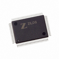
Z16F2810FI20EG Zilog, Z16F2810FI20EG Datasheet - Page 199

Z16F2810FI20EG
Manufacturer Part Number
Z16F2810FI20EG
Description
IC ZNEO MCU FLASH 128K 80QFP
Manufacturer
Zilog
Series
Encore!® ZNEOr
Datasheet
1.Z16F2800100ZCOG.pdf
(388 pages)
Specifications of Z16F2810FI20EG
Core Processor
ZNEO
Core Size
16-Bit
Speed
20MHz
Connectivity
I²C, IrDA, LIN, SPI, UART/USART
Peripherals
Brown-out Detect/Reset, DMA, POR, PWM, WDT
Number Of I /o
60
Program Memory Size
128KB (128K x 8)
Program Memory Type
FLASH
Ram Size
4K x 8
Voltage - Supply (vcc/vdd)
2.7 V ~ 3.6 V
Data Converters
A/D 12x10b
Oscillator Type
Internal
Operating Temperature
-40°C ~ 105°C
Package / Case
80-BQFP
Data Bus Width
16 bit
Data Ram Size
4 B
Interface Type
ESPI, I2C, UART
Maximum Clock Frequency
20 MHz
Number Of Programmable I/os
60
Number Of Timers
4
Operating Supply Voltage
2.7 V to 3.6 V
Maximum Operating Temperature
+ 105 C
Mounting Style
SMD/SMT
Minimum Operating Temperature
- 40 C
On-chip Adc
10 bit, 12 Channel
For Use With
770-1003 - ISP 4PORT FOR ZILOG ZNEO MCU269-4537 - DEV KIT FOR Z16F ZNEO
Lead Free Status / RoHS Status
Lead free / RoHS Compliant
Eeprom Size
-
Lead Free Status / Rohs Status
Details
Available stocks
Company
Part Number
Manufacturer
Quantity
Price
- Current page: 199 of 388
- Download datasheet (22Mb)
®
ZNEO
Z16F Series
Product Specification
183
software, is to set the
bit of the transmit data command register when the last TDRE
TEOF
interrupt or DMA request is being serviced (set TEOF before or simultaneously with
writing the last data byte). When the last bit of the last character is transmitted, the
hardware will automatically deassert the SSV and TEOF bits. The second method is for
software to directly clear the SSV bit after the transaction completes. If software clears the
SSV bit directly, it is not necessary for software to also set the TEOF bit on the last
transmit byte. After writing the last transmit byte, the end of the transaction is detected by
waiting for the last RDRF interrupt or monitoring the TFST bit in the ESPI Status register.
The transmit underrun and receive overrun errors do not occur in an SPI mode master. If
the RDRF and TDRE requests have not been serviced before the current byte transfer
completes, SCLK is paused until the data register is read and written. The transmit
underrun and receive overrun errors will occur in a slave if the slave’s software/DMA does
not keep up with the master data rate. If a transmit underrun occurs in SLAVE mode, the
shift register in the slave is loaded with all 1s.
In the SPI mode, the SCK is active only for the data transfer with one SCK period per bit
transferred. If the SPI bus has multiple slaves, the slave select lines to all or one of the
slaves must be controlled independently by software using GPIO pins.
Figure 37
on page 184 displays multiple character transfer in SPI mode. Note that while
character ’n’ is being transferred using the shift register, software/DMA responds to the
receive request for character n-1 and the transmit request for character n+1.
PS022008-0810
P R E L I M I N A R Y
Enhanced Serial Peripheral Interface
Related parts for Z16F2810FI20EG
Image
Part Number
Description
Manufacturer
Datasheet
Request
R

Part Number:
Description:
Communication Controllers, ZILOG INTELLIGENT PERIPHERAL CONTROLLER (ZIP)
Manufacturer:
Zilog, Inc.
Datasheet:

Part Number:
Description:
KIT DEV FOR Z8 ENCORE 16K TO 64K
Manufacturer:
Zilog
Datasheet:

Part Number:
Description:
KIT DEV Z8 ENCORE XP 28-PIN
Manufacturer:
Zilog
Datasheet:

Part Number:
Description:
DEV KIT FOR Z8 ENCORE 8K/4K
Manufacturer:
Zilog
Datasheet:

Part Number:
Description:
KIT DEV Z8 ENCORE XP 28-PIN
Manufacturer:
Zilog
Datasheet:

Part Number:
Description:
DEV KIT FOR Z8 ENCORE 4K TO 8K
Manufacturer:
Zilog
Datasheet:

Part Number:
Description:
CMOS Z8 microcontroller. ROM 16 Kbytes, RAM 256 bytes, speed 16 MHz, 32 lines I/O, 3.0V to 5.5V
Manufacturer:
Zilog, Inc.
Datasheet:

Part Number:
Description:
Low-cost microcontroller. 512 bytes ROM, 61 bytes RAM, 8 MHz
Manufacturer:
Zilog, Inc.
Datasheet:

Part Number:
Description:
Z8 4K OTP Microcontroller
Manufacturer:
Zilog, Inc.
Datasheet:

Part Number:
Description:
CMOS SUPER8 ROMLESS MCU
Manufacturer:
Zilog, Inc.
Datasheet:

Part Number:
Description:
SL1866 CMOSZ8 OTP Microcontroller
Manufacturer:
Zilog, Inc.
Datasheet:

Part Number:
Description:
SL1866 CMOSZ8 OTP Microcontroller
Manufacturer:
Zilog, Inc.
Datasheet:

Part Number:
Description:
OTP (KB) = 1, RAM = 125, Speed = 12, I/O = 14, 8-bit Timers = 2, Comm Interfaces Other Features = Por, LV Protect, Voltage = 4.5-5.5V
Manufacturer:
Zilog, Inc.
Datasheet:

Part Number:
Description:
Manufacturer:
Zilog, Inc.
Datasheet:


