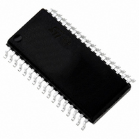
ST72F63BK4M1 STMicroelectronics, ST72F63BK4M1 Datasheet - Page 43

ST72F63BK4M1
Manufacturer Part Number
ST72F63BK4M1
Description
IC MCU 8BIT LS 16K 34-SOIC
Manufacturer
STMicroelectronics
Series
ST7r
Datasheet
1.ST72F63BD6U1TR.pdf
(186 pages)
Specifications of ST72F63BK4M1
Core Processor
ST7
Core Size
8-Bit
Speed
8MHz
Connectivity
I²C, SCI, USB
Peripherals
DMA, LVD, POR, PWM, WDT
Number Of I /o
19
Program Memory Size
16KB (16K x 8)
Program Memory Type
FLASH
Ram Size
512 x 8
Voltage - Supply (vcc/vdd)
4 V ~ 5.5 V
Data Converters
A/D 8x8b
Oscillator Type
Internal
Operating Temperature
0°C ~ 70°C
Package / Case
34-SOIC (7.5mm Width)
Processor Series
ST72F6x
Core
ST7
Data Bus Width
8 bit
Data Ram Size
512 B
Interface Type
I2C, SCI, USB
Maximum Clock Frequency
8 MHz
Number Of Programmable I/os
27
Number Of Timers
2 x 16 bit
Operating Supply Voltage
4 V to 5.5 V
Maximum Operating Temperature
+ 70 C
Mounting Style
SMD/SMT
Development Tools By Supplier
ST7MDTU3-EPB/US, ST72F63B-SK/RAIS, ST7MDTU3-EMU3, STX-RLINK
Minimum Operating Temperature
0 C
On-chip Adc
8 bit
For Use With
497-5521 - EVAL BOARD LOW SPEED USB
Lead Free Status / RoHS Status
Lead free / RoHS Compliant
Eeprom Size
-
Lead Free Status / Rohs Status
Details
Other names
497-2115-5
Available stocks
Company
Part Number
Manufacturer
Quantity
Price
Part Number:
ST72F63BK4M1
Manufacturer:
ST
Quantity:
20 000
ST7263Bxx
9
9.1
9.2
Note:
1
2
I/O ports
Introduction
The I/O ports offer different functional modes:
●
●
●
●
An I/O port consists of up to 8 pins. Each pin can be programmed independently as a digital
input (with or without interrupt generation) or a digital output.
Functional description
Each port is associated to 2 main registers:
●
●
Each I/O pin may be programmed using the corresponding register bits in DDR register: bit
X corresponding to pin X of the port. The same correspondence is used for the DR register.
Table 10.
Input modes
The input configuration is selected by clearing the corresponding DDR register bit.
In this case, reading the DR register returns the digital value applied to the external I/O pin.
All the inputs are triggered by a Schmitt trigger.
When switching from input mode to output mode, the DR register should be written first to
output the correct value as soon as the port is configured as an output.
Interrupt function
When an I/O is configured as an input with interrupt, an event on this I/O can generate an
external interrupt request to the CPU. The interrupt sensitivity is given independently
according to the description mentioned in the ITRFRE interrupt register.
Each pin can independently generate an interrupt request.
Each external interrupt vector is linked to a dedicated group of I/O port pins (see interrupts
section). If more than one input pin is selected simultaneously as an interrupt source, this is
logically ORed. For this reason if one of the interrupt pins is tied low, the other ones are
masked.
Transfer of data through digital inputs and outputs and for specific pins
Analog signal input (ADC)
Alternate signal input/output for the on-chip peripherals
External interrupt generation
Data register (DR)
Data Direction register (DDR)
I/O pin functions
DDR
0
1
Doc ID 7516 Rev 8
Output
Mode
Input
I/O ports
43/186


