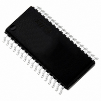
ST72F63BK4M1 STMicroelectronics, ST72F63BK4M1 Datasheet - Page 112

ST72F63BK4M1
Manufacturer Part Number
ST72F63BK4M1
Description
IC MCU 8BIT LS 16K 34-SOIC
Manufacturer
STMicroelectronics
Series
ST7r
Datasheet
1.ST72F63BD6U1TR.pdf
(186 pages)
Specifications of ST72F63BK4M1
Core Processor
ST7
Core Size
8-Bit
Speed
8MHz
Connectivity
I²C, SCI, USB
Peripherals
DMA, LVD, POR, PWM, WDT
Number Of I /o
19
Program Memory Size
16KB (16K x 8)
Program Memory Type
FLASH
Ram Size
512 x 8
Voltage - Supply (vcc/vdd)
4 V ~ 5.5 V
Data Converters
A/D 8x8b
Oscillator Type
Internal
Operating Temperature
0°C ~ 70°C
Package / Case
34-SOIC (7.5mm Width)
Processor Series
ST72F6x
Core
ST7
Data Bus Width
8 bit
Data Ram Size
512 B
Interface Type
I2C, SCI, USB
Maximum Clock Frequency
8 MHz
Number Of Programmable I/os
27
Number Of Timers
2 x 16 bit
Operating Supply Voltage
4 V to 5.5 V
Maximum Operating Temperature
+ 70 C
Mounting Style
SMD/SMT
Development Tools By Supplier
ST7MDTU3-EPB/US, ST72F63B-SK/RAIS, ST7MDTU3-EMU3, STX-RLINK
Minimum Operating Temperature
0 C
On-chip Adc
8 bit
For Use With
497-5521 - EVAL BOARD LOW SPEED USB
Lead Free Status / RoHS Status
Lead free / RoHS Compliant
Eeprom Size
-
Lead Free Status / Rohs Status
Details
Other names
497-2115-5
Available stocks
Company
Part Number
Manufacturer
Quantity
Price
Part Number:
ST72F63BK4M1
Manufacturer:
ST
Quantity:
20 000
On-chip peripherals
Note:
112/186
Following the address reception and after SR1 register has been read, the slave receives
bytes from the SDA line into the DR register via the internal shift register. After each byte the
interface generates in sequence:
●
●
Then the interface waits for a read of the SR1 register followed by a read of the DR register,
holding the SCL line low (see
Slave transmitter
Following the address reception and after the SR1 register has been read, the slave sends
bytes from the DR register to the SDA line via the internal shift register.
The slave waits for a read of the SR1 register followed by a write in the DR register, holding
the SCL line low (see
When the acknowledge pulse is received, the EVF and BTF bits are set by hardware with an
interrupt if the ITE bit is set.
Closing Slave communication
After the last data byte is transferred a Stop Condition is generated by the master. The
interface detects this condition and sets EVF and STOPF bits with an interrupt if the ITE bit
is set.
Then the interface waits for a read of the SR2 register (see
EV4).
Error cases
●
●
In case of errors, SCL line is not held low; however, the SDA line can remain low if the last
bits transmitted are all 0. While AF=1, the SCL line may be held low due to SB or BTF flags
that are set at the same time. It is then necessary to release both lines by software.
How to Release the SDA / SCL lines
Set and subsequently clear the STOP bit while BTF is set. The SDA/SCL lines are released
after the transfer of the current byte.
Master mode
To switch from default Slave mode to Master mode, a Start condition generation is needed.
Start condition
Acknowledge pulse if the ACK bit is set
EVF and BTF bits are set with an interrupt if the ITE bit is set.
BERR: Detection of a Stop or a Start condition during a byte transfer. In this case, the
EVF and the BERR bits are set with an interrupt if the ITE bit is set.
If it is a Stop, then the interface discards the data, released the lines and waits for
another Start condition.
If it is a Start, then the interface discards the data and waits for the next slave address
on the bus.
AF: Detection of a non-acknowledge bit. In this case, the EVF and AF bits are set with
an interrupt if the ITE bit is set.
The AF bit is cleared by reading the I2CSR2 register. However, if read before the
completion of the transmission, the AF flag will be set again, thus possibly generating a
new interrupt. Software must ensure either that the SCL line is back at 0 before reading
the SR2 register, or be able to correctly handle a second interrupt during the 9th pulse
of a transmitted byte.
Figure 48
Doc ID 7516 Rev 8
Figure 48
Transfer sequencing EV3).
Transfer sequencing EV2).
Figure 48
Transfer sequencing
ST7263Bxx


