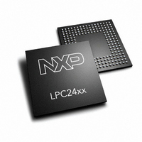
LPC2460FET208,551 NXP Semiconductors, LPC2460FET208,551 Datasheet - Page 191

LPC2460FET208,551
Manufacturer Part Number
LPC2460FET208,551
Description
IC ARM7 MCU ROMLESS 208TFBGA
Manufacturer
NXP Semiconductors
Series
LPC2400r
Specifications of LPC2460FET208,551
Program Memory Type
ROMless
Package / Case
208-TFBGA
Core Processor
ARM7
Core Size
16/32-Bit
Speed
72MHz
Connectivity
CAN, EBI/EMI, Ethernet, I²C, Microwire, MMC, SPI, SSI, SSP, UART/USART, USB OTG
Peripherals
Brown-out Detect/Reset, DMA, I²S, POR, PWM, WDT
Number Of I /o
160
Ram Size
96K x 8
Voltage - Supply (vcc/vdd)
3 V ~ 3.6 V
Data Converters
A/D 8x10b; D/A 1x10b
Oscillator Type
Internal
Operating Temperature
-40°C ~ 85°C
Processor Series
LPC24
Core
ARM7TDMI-S
Data Bus Width
16 bit, 32 bit
Data Ram Size
98 KB
Interface Type
CAN/I2C/I2S/SPI/SSP/UART/USB
Maximum Clock Frequency
72 MHz
Number Of Programmable I/os
160
Number Of Timers
4
Operating Supply Voltage
3.3 V
Maximum Operating Temperature
+ 85 C
Mounting Style
SMD/SMT
3rd Party Development Tools
MDK-ARM, RL-ARM, ULINK2, MCB2460, MCB2460U
Minimum Operating Temperature
- 40 C
On-chip Adc
8-ch x 10-bit
On-chip Dac
1-ch x 10-bit
Lead Free Status / RoHS Status
Lead free / RoHS Compliant
For Use With
MCB2400U - BOARD EVAL MCB2400 + ULINK2MCB2400 - BOARD EVAL FOR NXP LPC246X SER
Eeprom Size
-
Program Memory Size
-
Lead Free Status / Rohs Status
Lead free / RoHS Compliant
Other names
568-4260
935283232551
LPC2460FET208-S
935283232551
LPC2460FET208-S
Available stocks
Company
Part Number
Manufacturer
Quantity
Price
Company:
Part Number:
LPC2460FET208,551
Manufacturer:
NXP Semiconductors
Quantity:
10 000
- Current page: 191 of 792
- Download datasheet (5Mb)
NXP Semiconductors
UM10237_4
User manual
5.14 Pin Mode select register 1 (PINMODE1 - 0xE002 C044)
5.15 Pin Mode select register 2 (PINMODE2 - 0xE002 C048)
5.16 Pin Mode select register 3 (PINMODE3 - 0xE002 C04C)
5.17 Pin Mode select register 4 (PINMODE4 - 0xE002 C050)
This register controls pull-up/pull-down resistor configuration for PORT0 pins 16 to 26. For
details see
Table 147. Pin Mode select register 1 (PINMODE1 - address 0xE002 C044) bit description
Remark: Pins P0.27 and P0.28 are dedicated I
Pins P0.29, P0.30, P0.31 are USB specific pins without configurable pull-up or pull-down
resistors.
This register controls pull-up/pull-down resistor configuration for PORT1 pins 0 to 15. For
details see
Table 148. Pin Mode select register 2 (PINMODE2 - address 0xE002 C048) bit description
This register controls pull-up/pull-down resistor configuration for PORT1 pins 16 to 31. For
details see
Table 149. Pin Mode select register 3 (PINMODE3 - address 0xE002 C04C) bit description
This register controls pull-up/pull-down resistor configuration for PORT2 pins 0 to 15. For
details see
PINMODE1 Symbol
1:0
...
21:20
31:21
PINMODE2 Symbol
1:0
...
31:30
PINMODE3 Symbol
1:0
...
31:30
Section 9–4 “Pin mode select register
Section 9–4 “Pin mode select register
Section 9–4 “Pin mode select register
Section 9–4 “Pin mode select register
P0.16MODE
P0.26MODE
-
P1.00MODE
P1.15MODE
P1.16MODE
P1.31MODE
Rev. 04 — 26 August 2009
Description
PORT0 pin 16 on-chip pull-up/down resistor control.
PORT0 pin 26 on-chip pull-up/down resistor control.
Reserved
Description
PORT1 pin 0 on-chip pull-up/down resistor control.
PORT1 pin 15 on-chip pull-up/down resistor control.
Description
PORT1 pin 16 on-chip pull-up/down resistor control.
PORT1 pin 31 on-chip pull-up/down resistor control.
2
C open drain pins without pull-up/down.
values”.
values”.
values”.
values”.
Chapter 9: LPC24XX Pin connect
UM10237
© NXP B.V. 2009. All rights reserved.
191 of 792
Reset
value
00
00
Reset
value
00
00
Reset
value
00
00
Related parts for LPC2460FET208,551
Image
Part Number
Description
Manufacturer
Datasheet
Request
R
Part Number:
Description:
Flashless 16-bit/32-bit Micro; Ethernet, Can, Isp/iap, Usb 2.0 Device/host/otg, External Memory Interface
Manufacturer:
NXP Semiconductors
Datasheet:

Part Number:
Description:
MCU, MPU & DSP Development Tools EVAL BOARD FOR NXP LPC246x
Manufacturer:
Keil Tools
Part Number:
Description:
NXP Semiconductors designed the LPC2420/2460 microcontroller around a 16-bit/32-bitARM7TDMI-S CPU core with real-time debug interfaces that include both JTAG andembedded trace
Manufacturer:
NXP Semiconductors
Datasheet:

Part Number:
Description:
NXP Semiconductors designed the LPC2458 microcontroller around a 16-bit/32-bitARM7TDMI-S CPU core with real-time debug interfaces that include both JTAG andembedded trace
Manufacturer:
NXP Semiconductors
Datasheet:
Part Number:
Description:
NXP Semiconductors designed the LPC2468 microcontroller around a 16-bit/32-bitARM7TDMI-S CPU core with real-time debug interfaces that include both JTAG andembedded trace
Manufacturer:
NXP Semiconductors
Datasheet:
Part Number:
Description:
NXP Semiconductors designed the LPC2470 microcontroller, powered by theARM7TDMI-S core, to be a highly integrated microcontroller for a wide range ofapplications that require advanced communications and high quality graphic displays
Manufacturer:
NXP Semiconductors
Datasheet:
Part Number:
Description:
NXP Semiconductors designed the LPC2478 microcontroller, powered by theARM7TDMI-S core, to be a highly integrated microcontroller for a wide range ofapplications that require advanced communications and high quality graphic displays
Manufacturer:
NXP Semiconductors
Datasheet:
Part Number:
Description:
The Philips Semiconductors XA (eXtended Architecture) family of 16-bit single-chip microcontrollers is powerful enough to easily handle the requirements of high performance embedded applications, yet inexpensive enough to compete in the market for hi
Manufacturer:
NXP Semiconductors
Datasheet:
Part Number:
Description:
The XA-S3 device is a member of Philips Semiconductors? XA(eXtended Architecture) family of high performance 16-bitsingle-chip microcontrollers
Manufacturer:
NXP Semiconductors
Datasheet:

Part Number:
Description:
The NXP BlueStreak LH75401/LH75411 family consists of two low-cost 16/32-bit System-on-Chip (SoC) devices
Manufacturer:
NXP Semiconductors
Datasheet:

Part Number:
Description:
The NXP LPC3130/3131 combine an 180 MHz ARM926EJ-S CPU core, high-speed USB2
Manufacturer:
NXP Semiconductors
Datasheet:

Part Number:
Description:
The NXP LPC3141 combine a 270 MHz ARM926EJ-S CPU core, High-speed USB 2
Manufacturer:
NXP Semiconductors

Part Number:
Description:
The NXP LPC3143 combine a 270 MHz ARM926EJ-S CPU core, High-speed USB 2
Manufacturer:
NXP Semiconductors

Part Number:
Description:
The NXP LPC3152 combines an 180 MHz ARM926EJ-S CPU core, High-speed USB 2
Manufacturer:
NXP Semiconductors


