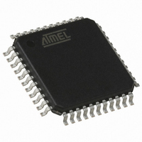
AT89C51CC03CA-RLTUM Atmel, AT89C51CC03CA-RLTUM Datasheet - Page 58

AT89C51CC03CA-RLTUM
Manufacturer Part Number
AT89C51CC03CA-RLTUM
Description
IC 8051 MCU 64K FLASH 44-VQFP
Manufacturer
Atmel
Series
AT89C CANr
Datasheet
1.AT89C51CC03C-S3RIM.pdf
(198 pages)
Specifications of AT89C51CC03CA-RLTUM
Core Processor
8051
Core Size
8-Bit
Speed
40MHz
Connectivity
CAN, UART/USART
Peripherals
POR, PWM, WDT
Number Of I /o
36
Program Memory Size
64KB (64K x 8)
Program Memory Type
FLASH
Eeprom Size
2K x 8
Ram Size
2.25K x 8
Voltage - Supply (vcc/vdd)
3 V ~ 5.5 V
Data Converters
A/D 8x10b
Oscillator Type
External
Operating Temperature
-40°C ~ 85°C
Package / Case
44-TQFP, 44-VQFP
Processor Series
AT89x
Core
8051
Data Bus Width
8 bit
Data Ram Size
2304 B
Interface Type
UART, SPI
Maximum Clock Frequency
60 MHz
Number Of Programmable I/os
36
Number Of Timers
2
Operating Supply Voltage
3 V to 5.5 V
Maximum Operating Temperature
+ 85 C
Mounting Style
SMD/SMT
3rd Party Development Tools
PK51, CA51, A51, ULINK2
Minimum Operating Temperature
- 40 C
On-chip Adc
10 bit, 8 Channel
Package
44VQFP
Device Core
8051
Family Name
AT89
Maximum Speed
60 MHz
For Use With
AT89OCD-01 - USB EMULATOR FOR AT8XC51 MCU
Lead Free Status / RoHS Status
Lead free / RoHS Compliant
Available stocks
Company
Part Number
Manufacturer
Quantity
Price
Company:
Part Number:
AT89C51CC03CA-RLTUM
Manufacturer:
ADI
Quantity:
141
In-System
Programming (ISP)
Flash Programming and
Erasure
Boot Process
Software Boot Process
Example
58
AT89C51CC03
With the implementation of the User Space (FM0) and the Boot Space (FM1) in Flash
technology the AT89C51CC03 allows the system engineer the development of applica-
tions with a very high level of flexibility. This flexibility is based on the possibility to alter
the customer program at any stages of a product’s life:
•
•
This In-System Programming (ISP) allows code modification over the total lifetime of the
product.
Besides the default Boot loader Atmel provide to the customer also all the needed Appli-
cation-Programming-Interfaces (API) which are needed for the ISP. The API are located
also in the Boot memory.
This allow the customer to have a full use of the 64-Kbyte user memory.
There are three methods of programming the Flash memory:
•
•
•
Figure 29. Flash Memory Mapping
Many algorithms can be used for the software boot process. Before describing them,
The description of the different flags and Bytes is given below:
Before assembly the 1st personalization of the product by programming in the FM0
and if needed also a customized Boot loader in the FM1.
Atmel provide also a standard Boot loader by default UART or CAN.
After assembling on the PCB in its final embedded position by serial mode via the
CAN bus or UART.
The Atmel bootloader located in FM1 is activated by the application. Low level API
routines (located in FM1)will be used to program FM0. The interface used for serial
downloading to FM0 is the UART or the CAN. API can be called also by the user’s
bootloader located in FM0 at [SBV]00h.
A further method exists in activating the Atmel boot loader by hardware activation.
The FM0 can be programmed also by the parallel mode using a programmer.
[SBV]00h
FFFFh
0000h
Flash memory
64K Bytes
Custom
Boot Loader
FM0
F800h
FM1 mapped between F800h and FFFFh
when API called
2K Bytes IAP
bootloader
FM1
FFFFh
4182O–CAN–09/08


