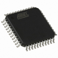
AT89C51CC03CA-RLTUM Atmel, AT89C51CC03CA-RLTUM Datasheet - Page 53

AT89C51CC03CA-RLTUM
Manufacturer Part Number
AT89C51CC03CA-RLTUM
Description
IC 8051 MCU 64K FLASH 44-VQFP
Manufacturer
Atmel
Series
AT89C CANr
Datasheet
1.AT89C51CC03C-S3RIM.pdf
(198 pages)
Specifications of AT89C51CC03CA-RLTUM
Core Processor
8051
Core Size
8-Bit
Speed
40MHz
Connectivity
CAN, UART/USART
Peripherals
POR, PWM, WDT
Number Of I /o
36
Program Memory Size
64KB (64K x 8)
Program Memory Type
FLASH
Eeprom Size
2K x 8
Ram Size
2.25K x 8
Voltage - Supply (vcc/vdd)
3 V ~ 5.5 V
Data Converters
A/D 8x10b
Oscillator Type
External
Operating Temperature
-40°C ~ 85°C
Package / Case
44-TQFP, 44-VQFP
Processor Series
AT89x
Core
8051
Data Bus Width
8 bit
Data Ram Size
2304 B
Interface Type
UART, SPI
Maximum Clock Frequency
60 MHz
Number Of Programmable I/os
36
Number Of Timers
2
Operating Supply Voltage
3 V to 5.5 V
Maximum Operating Temperature
+ 85 C
Mounting Style
SMD/SMT
3rd Party Development Tools
PK51, CA51, A51, ULINK2
Minimum Operating Temperature
- 40 C
On-chip Adc
10 bit, 8 Channel
Package
44VQFP
Device Core
8051
Family Name
AT89
Maximum Speed
60 MHz
For Use With
AT89OCD-01 - USB EMULATOR FOR AT8XC51 MCU
Lead Free Status / RoHS Status
Lead free / RoHS Compliant
Available stocks
Company
Part Number
Manufacturer
Quantity
Price
Company:
Part Number:
AT89C51CC03CA-RLTUM
Manufacturer:
ADI
Quantity:
141
Power Down Request
Reading the Flash Spaces
User
Extra Row
Hardware Security Byte
Flash Protection from Parallel
Programming
4182O–CAN–09/08
Before entering in Power Down (Set bit PD in PCON register) the user should check that
no write sequence is in progress (check BUSY=0), then check that the column latches
are reset (FLOAD=0 in FSTA register. Launch a reset column latches to clear FLOAD if
necessary.
The following procedure is used to read the User space:
•
Note:
The following procedure is used to read the Extra Row space and is summarized in
Figure 28:
•
•
•
The following procedure is used to read the Hardware
summarized in Figure 28:
•
•
Figure 28. Clear FCON to unmap the Hardware Security Byte.Reading Procedure
The three lock bits in Hardware Security Byte (see "In-System Programming" section)
are programmed according to Table 17 provide different level of protection for the on-
chip code and data located in FM0 and FM1.
The only way to write this bits are the parallel mode. They are set by default to level 4
Read one byte in Accumulator by executing MOVC A,@A+DPTR with
A+DPTR=read@.
Map the Extra Row space by writing 02h in FCON register.
Read one byte in Accumulator by executing MOVC A,@A+DPTR with A = 0 and
DPTR = FF80h to FFFFh.
Clear FCON to unmap the Extra Row.
Map the Hardware Security space by writing 04h in FCON register.
Read the byte in Accumulator by executing MOVC A,@A+DPTR with A = 0 and
DPTR = 0000h.
FCON is supposed to be reset when not needed.
Exec: MOVC A, @A+DPTR
Flash Spaces Reading
Flash Spaces Mapping
FCON= 00000xx0b
DPTR= Address
FCON = 00h
Clear Mode
Data Read
ACC= 0
AT89C51CC03
Security
space and is
53


