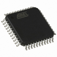
AT89C51CC03CA-RLTUM Atmel, AT89C51CC03CA-RLTUM Datasheet - Page 48

AT89C51CC03CA-RLTUM
Manufacturer Part Number
AT89C51CC03CA-RLTUM
Description
IC 8051 MCU 64K FLASH 44-VQFP
Manufacturer
Atmel
Series
AT89C CANr
Datasheet
1.AT89C51CC03C-S3RIM.pdf
(198 pages)
Specifications of AT89C51CC03CA-RLTUM
Core Processor
8051
Core Size
8-Bit
Speed
40MHz
Connectivity
CAN, UART/USART
Peripherals
POR, PWM, WDT
Number Of I /o
36
Program Memory Size
64KB (64K x 8)
Program Memory Type
FLASH
Eeprom Size
2K x 8
Ram Size
2.25K x 8
Voltage - Supply (vcc/vdd)
3 V ~ 5.5 V
Data Converters
A/D 8x10b
Oscillator Type
External
Operating Temperature
-40°C ~ 85°C
Package / Case
44-TQFP, 44-VQFP
Processor Series
AT89x
Core
8051
Data Bus Width
8 bit
Data Ram Size
2304 B
Interface Type
UART, SPI
Maximum Clock Frequency
60 MHz
Number Of Programmable I/os
36
Number Of Timers
2
Operating Supply Voltage
3 V to 5.5 V
Maximum Operating Temperature
+ 85 C
Mounting Style
SMD/SMT
3rd Party Development Tools
PK51, CA51, A51, ULINK2
Minimum Operating Temperature
- 40 C
On-chip Adc
10 bit, 8 Channel
Package
44VQFP
Device Core
8051
Family Name
AT89
Maximum Speed
60 MHz
For Use With
AT89OCD-01 - USB EMULATOR FOR AT8XC51 MCU
Lead Free Status / RoHS Status
Lead free / RoHS Compliant
Available stocks
Company
Part Number
Manufacturer
Quantity
Price
Company:
Part Number:
AT89C51CC03CA-RLTUM
Manufacturer:
ADI
Quantity:
141
Status of the Flash Memory
Selecting FM1
Loading the Column Latches
48
AT89C51CC03
Table 16. Programming Spaces
Notes:
The bit FBUSY in FCON register is used to indicate the status of programming.
FBUSY is set when programming is in progress.
The flash programming process is launched the second machine cycle following the
sequence 5xh and Axh in FCON. Thus the FBUSY flag should be read by sofware not
during the insctruction after the 5xh, Axh sequence but the the second instruction after
the 5xh, Axh sequence in FCON (See next example). FBUSY is cleared when the pro-
gramming is completed.
The bit ENBOOT in AUXR1 register is used to map FM1 from F800h to FFFFh.
Any number of data from 1-byte to 128 Bytes can be loaded in the column latches. This
provides the capability to program the whole memory by byte, by page or by any number
of Bytes in a page. Data written in the column latches do not have to be in consecutive
Extra Row
Hardware
Columns
Security
Latches
Reset
User
Byte
;*F*************************************************************************
;* NAME: launch_prog
;;***************************************************************************
launch_prog:
wait_busy:
1. The sequence 5xh and Axh must be executing without instructions between them
2. The sequence 5xh and Axh must be executed with the same FMOD0 FMOD1
3. Interrupts that may occur during programming time must be disabled to avoid any
MOV FCON, #050h
MOV FCON #0A0h ; Flash Write Sequence
NOP
MOV A,FCON
JB ACC.0,wait_busy
RET
otherwise the programming is not executed (see Flash Status Register)
configuration.
spurious exit of the programming mode.
FPL3:0
A
A
A
A
5
5
5
5
FPS
;Required time before reading busy flag
Write to FCON
X
X
X
X
X
X
X
X
FMOD1
0
0
0
0
1
1
1
1
FMOD0
0
0
1
1
0
0
1
1
Operation
No action
Write the column latches in user
space
No action
Write the column latches in extra row
space
No action
Write the fuse bits space
No action
Reset the column latches
4182O–CAN–09/08


