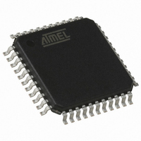
AT89C51CC03CA-RLTUM Atmel, AT89C51CC03CA-RLTUM Datasheet - Page 42

AT89C51CC03CA-RLTUM
Manufacturer Part Number
AT89C51CC03CA-RLTUM
Description
IC 8051 MCU 64K FLASH 44-VQFP
Manufacturer
Atmel
Series
AT89C CANr
Datasheet
1.AT89C51CC03C-S3RIM.pdf
(198 pages)
Specifications of AT89C51CC03CA-RLTUM
Core Processor
8051
Core Size
8-Bit
Speed
40MHz
Connectivity
CAN, UART/USART
Peripherals
POR, PWM, WDT
Number Of I /o
36
Program Memory Size
64KB (64K x 8)
Program Memory Type
FLASH
Eeprom Size
2K x 8
Ram Size
2.25K x 8
Voltage - Supply (vcc/vdd)
3 V ~ 5.5 V
Data Converters
A/D 8x10b
Oscillator Type
External
Operating Temperature
-40°C ~ 85°C
Package / Case
44-TQFP, 44-VQFP
Processor Series
AT89x
Core
8051
Data Bus Width
8 bit
Data Ram Size
2304 B
Interface Type
UART, SPI
Maximum Clock Frequency
60 MHz
Number Of Programmable I/os
36
Number Of Timers
2
Operating Supply Voltage
3 V to 5.5 V
Maximum Operating Temperature
+ 85 C
Mounting Style
SMD/SMT
3rd Party Development Tools
PK51, CA51, A51, ULINK2
Minimum Operating Temperature
- 40 C
On-chip Adc
10 bit, 8 Channel
Package
44VQFP
Device Core
8051
Family Name
AT89
Maximum Speed
60 MHz
For Use With
AT89OCD-01 - USB EMULATOR FOR AT8XC51 MCU
Lead Free Status / RoHS Status
Lead free / RoHS Compliant
Available stocks
Company
Part Number
Manufacturer
Quantity
Price
Company:
Part Number:
AT89C51CC03CA-RLTUM
Manufacturer:
ADI
Quantity:
141
- Current page: 42 of 198
- Download datasheet (3Mb)
Figure 22. External Code Fetch Waveforms
Flash Memory
Architecture
Figure 23. Flash Memory Architecture with ENBOOT=1 (boot mode)
42
AT89C51CC03
Extra Row (128 Bytes)
Hardware Security (1 byte)
Column Latches (128 Bytes)
CPU Clock
PSEN#
ALE
P0
P2
D7:0
PCH
AT89C51CC03 features two on-chip Flash memories:
•
•
The FM0 can be program by both parallel programming and Serial In-System Program-
ming (ISP) whereas FM1 supports only parallel programming by programmers. The ISP
mode is detailed in the "In-System Programming" section.
All Read/Write access operations on Flash Memory by user application are managed by
a set of API described in the "In-System Programming" section.
The bit ENBOOT in AUXR1 register is used to map FM1 from F800h to FFFFh. Figure
23 and Figure 24 show the Flash memory configuration with ENBOOT=1 and
ENBOOT=0.
FFFFh
F800h
0000h
Flash memory FM0:
containing 64K Bytes of program memory (user space) organized into 128 byte
pages,
Flash memory FM1:
2K Bytes for boot loader and Application Programming Interfaces (API).
PCL
64K Bytes
FM0
PCH
Memory space not accessible
D7:0
FM1 mapped between FFFFh and
F800h when bit ENBOOT is set in
AUXR1 register
PCL
Flash memory
boot space
2K Bytes
FM1
PCH
D7:0
FFFFh
F800h
4182O–CAN–09/08
Related parts for AT89C51CC03CA-RLTUM
Image
Part Number
Description
Manufacturer
Datasheet
Request
R

Part Number:
Description:
Manufacturer:
Atmel Corporation
Datasheet:

Part Number:
Description:
At89c51cc03 Enhanced 8-bit Mcu With Can Controller And Flash Memory
Manufacturer:
ATMEL Corporation
Datasheet:

Part Number:
Description:
DEV KIT FOR AVR/AVR32
Manufacturer:
Atmel
Datasheet:

Part Number:
Description:
INTERVAL AND WIPE/WASH WIPER CONTROL IC WITH DELAY
Manufacturer:
ATMEL Corporation
Datasheet:

Part Number:
Description:
Low-Voltage Voice-Switched IC for Hands-Free Operation
Manufacturer:
ATMEL Corporation
Datasheet:

Part Number:
Description:
MONOLITHIC INTEGRATED FEATUREPHONE CIRCUIT
Manufacturer:
ATMEL Corporation
Datasheet:

Part Number:
Description:
AM-FM Receiver IC U4255BM-M
Manufacturer:
ATMEL Corporation
Datasheet:

Part Number:
Description:
Monolithic Integrated Feature Phone Circuit
Manufacturer:
ATMEL Corporation
Datasheet:

Part Number:
Description:
Multistandard Video-IF and Quasi Parallel Sound Processing
Manufacturer:
ATMEL Corporation
Datasheet:

Part Number:
Description:
High-performance EE PLD
Manufacturer:
ATMEL Corporation
Datasheet:

Part Number:
Description:
8-bit Flash Microcontroller
Manufacturer:
ATMEL Corporation
Datasheet:

Part Number:
Description:
2-Wire Serial EEPROM
Manufacturer:
ATMEL Corporation
Datasheet:


