ATTINY48-MMU Atmel, ATTINY48-MMU Datasheet - Page 2
ATTINY48-MMU
Manufacturer Part Number
ATTINY48-MMU
Description
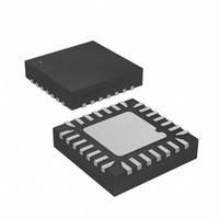
MCU AVR 5K FLASH 12MHZ 28-QFN
Manufacturer
Atmel
Series
AVR® ATtinyr
Specifications of ATTINY48-MMU
Core Processor
AVR
Core Size
8-Bit
Speed
12MHz
Connectivity
I²C, SPI
Peripherals
Brown-out Detect/Reset, POR, WDT
Number Of I /o
24
Program Memory Size
4KB (2K x 16)
Program Memory Type
FLASH
Eeprom Size
64 x 8
Ram Size
256 x 8
Voltage - Supply (vcc/vdd)
1.8 V ~ 5.5 V
Data Converters
A/D 6x10b
Oscillator Type
Internal
Operating Temperature
-40°C ~ 85°C
Package / Case
28-VQFN Exposed Pad, 28-HVQFN, 28-SQFN, 28-DHVQFN
Processor Series
ATTINY4x
Core
AVR8
Data Bus Width
8 bit
Data Ram Size
256 B
Interface Type
2-Wire, I2S, SPI
Maximum Clock Frequency
12 MHz
Number Of Programmable I/os
24
Number Of Timers
2
Maximum Operating Temperature
+ 85 C
Mounting Style
SMD/SMT
3rd Party Development Tools
EWAVR, EWAVR-BL
Development Tools By Supplier
ATAVRDRAGON, ATSTK500, ATSTK600, ATAVRISP2, ATAVRONEKIT
Minimum Operating Temperature
- 40 C
On-chip Adc
10 bit, 6 Channel
Package
28VQFN EP
Device Core
AVR
Family Name
ATtiny
Maximum Speed
12 MHz
Operating Supply Voltage
2.5|3.3|5 V
For Use With
ATAVRDRAGON - KIT DRAGON 32KB FLASH MEM AVR
Lead Free Status / RoHS Status
Lead free / RoHS Compliant


1. Pin Configurations
Figure 1-1.
2
ATtiny48/88
NOTE: Bottom pad should be soldered to ground.
Pinout of ATtiny48/88
(PCINT19/INT1) PD3
(PCINT19/INT1) PD3
(PCINT6/CLKI) PB6
(PCINT6/CLKI) PB6
(PCINT20/T0) PD4
(PCINT20/T0) PD4
(PCINT21/T1) PD5
(PCINT26) PA2
(PCINT27) PA3
(PCINT7) PB7
(PCINT7) PB7
Table 1-1.
A
B
C
D
E
F
GND
VCC
GND
VCC
1
2
3
4
5
6
7
8
1
2
3
4
5
6
7
28 MLF Top View
GND
VCC
TQFP Top View
PD2
PD3
PB6
PB7
1
32 UFBGA Top View. See
PD1
PD4
PD6
PD5
PA2
PA3
2
21
20
19
18
17
16
15
24
23
22
21
20
19
18
17
PC2 (ADC2/PCINT10)
PC1 (ADC1/PCINT9)
PC0 (ADC0/PCINT8)
GND
PC7 (PCI NT15)
AVCC
PB5 (SCK/PCINT5)
PC1 (ADC1/PCINT9)
PC0 (ADC0/PCINT8)
PA1 (ADC7/PCINT25)
GND
PC7 (PCINT15)
PA0 (ADC6/PCINT24)
AVCC
PB5 (SCK/PCINT5)
PD7
NOTE: Bottom pad should be soldered to ground.
PC6
PD0
PB0
3
PC4
PC5
PB2
PB1
(PCINT19/INT1) PD3
(PCINT6/CLKI) PB6
page
4
(PCINT20/T0) PD4
(PCINT26) PA2
(PCINT27) PA3
(PCINT7) PB7
288.
(PCINT0/CLKO/ICP1) PB0
GND
VCC
AVCC
(PCINT14/RESET) PC6
PC2
PC3
PC7
PB3
PA1
(PCINT18/INT0) PD2
(PCINT19/INT1) PD3
(PCINT22/AIN0) PD6
(PCINT23/AIN1) PD7
5
(PCINT6/CLKI) PB6
(PCINT20/T0) PD4
(PCINT21/T1) PD5
1
2
3
4
5
6
7
8
(PCINT16) PD0
(PCINT17) PD1
(PCINT7) PB7
32 MLF Top View
GND
VCC
GND
PC1
PC0
PB5
PB4
PA0
6
1
2
3
4
5
6
7
8
9
10
11
12
13
14
PDIP
28
27
26
25
24
23
22
21
20
19
18
17
16
15
24
23
22
21
20
19
18
17
PC5 (ADC5/SCL/PCINT13)
PC4 (ADC4/SDA/PCINT12)
PC3 (ADC3/PCINT11)
PC2 (ADC2/PCINT10)
PC1 (ADC1/PCINT9)
PC0 (ADC0/PCINT8)
GND
PC7 (PCINT15)
AVCC
PB5 (SCK/PCINT5)
PB4 (MISO/PCINT4)
PB3 (MOSI/PCINT3)
PB2 (SS/OC1B/PCINT2)
PB1 (OC1A/PCINT1)
PC1 (ADC1/PCINT9)
PC0 (ADC0/PCINT8)
PA1 (ADC7/PCINT25)
GND
PC7 (PCINT15)
PA0 (ADC6/PCINT24)
AVCC
PB5 (SCK/PCINT5)
8008G–AVR–04/11
Related parts for ATTINY48-MMU
Image
Part Number
Description
Manufacturer
Datasheet
Request
R

Part Number:
Description:
Manufacturer:
Atmel Corporation
Datasheet:

Part Number:
Description:
MCU AVR 4K ISP FLASH 1.8V 32TQFP
Manufacturer:
Atmel
Datasheet:

Part Number:
Description:
MCU AVR 4K ISP FLASH 1.8V 32-QFN
Manufacturer:
Atmel
Datasheet:

Part Number:
Description:
MCU AVR 4K ISP FLASH 1.8V 28-DIP
Manufacturer:
Atmel
Datasheet:

Part Number:
Description:
MCU AVR 4KB FLASH 12MHZ 32TQFP
Manufacturer:
Atmel
Datasheet:
Part Number:
Description:
MCU AVR 4KB FLASH 12MHZ 32QFN
Manufacturer:
Atmel
Datasheet:

Part Number:
Description:
MCU AVR 4KB FLASH 12MHZ 28-VQFN
Manufacturer:
Atmel
Datasheet:
Part Number:
Description:
MCU AVR 4KB FLASH 12MHZ 28QFN
Manufacturer:
Atmel
Datasheet:
Part Number:
Description:
8-bit Microcontrollers - MCU 4KB FL,64B EE, 256B SRAM-12MHz
Manufacturer:
Atmel
Part Number:
Description:
8-bit Microcontrollers - MCU Microcontroller
Manufacturer:
Atmel
Part Number:
Description:
Manufacturer:
Atmel Corporation
Datasheet: