MC56F8002VWL Freescale Semiconductor, MC56F8002VWL Datasheet - Page 68
MC56F8002VWL
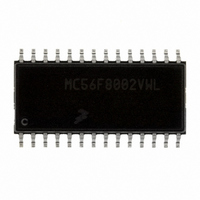
Manufacturer Part Number
MC56F8002VWL
Description
DSC 12K FLASH 32MHZ 28-SOIC
Manufacturer
Freescale Semiconductor
Series
56F8xxxr
Datasheet
1.MC56F8006DEMO.pdf
(100 pages)
Specifications of MC56F8002VWL
Core Processor
56800
Core Size
16-Bit
Speed
32MHz
Connectivity
I²C, LIN, SCI, SPI
Peripherals
LVD, POR, PWM, WDT
Number Of I /o
23
Program Memory Size
12KB (6K x 16)
Program Memory Type
FLASH
Ram Size
1K x 16
Voltage - Supply (vcc/vdd)
1.8 V ~ 3.6 V
Data Converters
A/D 15x12b
Oscillator Type
Internal
Operating Temperature
-40°C ~ 105°C
Package / Case
28-SOIC
Product
DSCs
Data Bus Width
16 bit
Processor Series
MC56F80xx
Core
56800E
Instruction Set Architecture
Dual Harvard
Device Million Instructions Per Second
32 MIPs
Maximum Clock Frequency
32 MHz
Number Of Programmable I/os
40
Data Ram Size
2 KB
Operating Supply Voltage
1.8 V to 3.6 V
Maximum Operating Temperature
+ 105 C
Mounting Style
SMD/SMT
Development Tools By Supplier
MC56F8006DEMO, APMOTOR56F8000E
Interface Type
LIN, I2C, SCI, SPI
Minimum Operating Temperature
- 40 C
For Use With
APMOTOR56F8000E - KIT DEMO MOTOR CTRL SYSTEM
Lead Free Status / RoHS Status
Lead free / RoHS Compliant
Eeprom Size
-
Lead Free Status / Rohs Status
Lead free / RoHS Compliant
Available stocks
Company
Part Number
Manufacturer
Quantity
Price

Part Number:
MC56F8002VWL
Manufacturer:
FREESCALE
Quantity:
20 000


Design Considerations
junction. The thermocouple wire is placed flat against the package case to avoid measurement errors caused by cooling effects
of the thermocouple wire.
When heat sink is used, the junction temperature is determined from a thermocouple inserted at the interface between the case
of the package and the interface material. A clearance slot or hole is normally required in the heat sink. Minimizing the size of
the clearance is important to minimize the change in thermal performance caused by removing part of the thermal interface to
the heat sink. Because of the experimental difficulties with this technique, many engineers measure the heat sink temperature
and then back-calculate the case temperature using a separate measurement of the thermal resistance of the interface. From this
case temperature, the junction temperature is determined from the junction-to-case thermal resistance.
9.2
Use the following list of considerations to assure correct operation of the 56F8006/56F8002:
68
•
•
•
•
•
•
•
•
•
•
•
•
•
•
•
•
Provide a low-impedance path from the board power supply to each V
board ground to each V
The minimum bypass requirement is to place 0.01–0.1µF capacitors positioned as near as possible to the package
supply pins. The recommended bypass configuration is to place one bypass capacitor on each of the V
including V
Ensure that capacitor leads and associated printed circuit traces that connect to the chip V
as short as possible.
Bypass the V
PCB trace lengths should be minimal for high-frequency signals.
Consider all device loads as well as parasitic capacitance due to PCB traces when calculating capacitance. This is
especially critical in systems with higher capacitive loads that could create higher transient currents in the V
V
Take special care to minimize noise levels on the V
Using separate power planes for V
Connect the separate analog and digital power and ground planes as near as possible to power supply outputs. If an
analog circuit and digital circuit are powered by the same power supply, you should connect a small inductor or ferrite
bead in serial with V
Physically separate analog components from noisy digital components by ground planes. Do not place an analog trace
in parallel with digital traces. Place an analog ground trace around an analog signal trace to isolate it from digital traces.
Because the flash memory is programmed through the JTAG/EOnCE port, SPI, SCI, or I
provide an interface to this port if in-circuit flash programming is desired.
If desired, connect an external RC circuit to the RESET pin. The resistor value should be in the range of 4.7 k –10 k ;
the capacitor value should be in the range of 0.22 µF–4.7 µF.
Configuring the RESET pin to GPIO output in normal operation in a high-noise environment may help to improve the
performance of noise transient immunity.
Add a 2.2 k external pullup on the TMS pin of the JTAG port to keep EOnCE in a restate during normal operation if
JTAG converter is not present.
During reset and after reset but before I/O initialization, all I/O pins are at input state with internal pullup enabled. The
typical value of internal pullup is around 33 k . These internal pullups can be disabled by software.
To eliminate PCB trace impedance effect, each ADC input should have a no less than 33 pF 10
External clamp diodes on analog input pins are recommended.
SS
Electrical Design Considerations
circuits.
This device contains protective circuitry to guard against damage due to high static voltage
or electrical fields. However, take normal precautions to avoid application of any voltages
higher than maximum-rated voltages to this high-impedance circuit. Reliability of
operation is enhanced if unused inputs are tied to an appropriate voltage level.
DDA
DD
/V
and V
SSA.
DDA
SS
Ceramic and tantalum capacitors tend to provide better tolerances.
SS
MC56F8006/MC56F8002 Digital Signal Controller, Rev. 3
and V
with approximately 100 µF, plus the number of 0.1 µF ceramic capacitors.
(GND) pin.
SSA
DD
traces.
and V
DDA
CAUTION
and separate ground planes for V
REF
, V
DDA
, and V
SSA
DD
pin on the 56F8006/56F8002 and from the
pins.
SS
and V
2
DD
C, the designer should
SSA
Freescale Semiconductor
and V
are recommended.
RC filter.
SS
(GND) pins are
DD
/V
SS
DD
pairs,
and
Related parts for MC56F8002VWL
Image
Part Number
Description
Manufacturer
Datasheet
Request
R

Part Number:
Description:
Manufacturer:
Freescale Semiconductor, Inc
Datasheet:
Part Number:
Description:
Manufacturer:
Freescale Semiconductor, Inc
Datasheet:
Part Number:
Description:
Manufacturer:
Freescale Semiconductor, Inc
Datasheet:
Part Number:
Description:
Manufacturer:
Freescale Semiconductor, Inc
Datasheet:
Part Number:
Description:
Manufacturer:
Freescale Semiconductor, Inc
Datasheet:
Part Number:
Description:
Manufacturer:
Freescale Semiconductor, Inc
Datasheet:
Part Number:
Description:
Manufacturer:
Freescale Semiconductor, Inc
Datasheet:
Part Number:
Description:
Manufacturer:
Freescale Semiconductor, Inc
Datasheet:
Part Number:
Description:
Manufacturer:
Freescale Semiconductor, Inc
Datasheet:
Part Number:
Description:
Manufacturer:
Freescale Semiconductor, Inc
Datasheet:
Part Number:
Description:
Manufacturer:
Freescale Semiconductor, Inc
Datasheet:
Part Number:
Description:
Manufacturer:
Freescale Semiconductor, Inc
Datasheet:
Part Number:
Description:
Manufacturer:
Freescale Semiconductor, Inc
Datasheet:
Part Number:
Description:
Manufacturer:
Freescale Semiconductor, Inc
Datasheet:
Part Number:
Description:
Manufacturer:
Freescale Semiconductor, Inc
Datasheet: