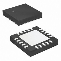
Z8F1233QH020SG Zilog, Z8F1233QH020SG Datasheet - Page 116

Z8F1233QH020SG
Manufacturer Part Number
Z8F1233QH020SG
Description
IC ENCORE XP MCU FLSH 12K 20QFN
Manufacturer
Zilog
Series
Encore!®r
Specifications of Z8F1233QH020SG
Core Processor
Z8
Core Size
8-Bit
Speed
20MHz
Peripherals
Brown-out Detect/Reset, LED, POR, PWM, WDT
Number Of I /o
17
Program Memory Size
12KB (12K x 8)
Program Memory Type
FLASH
Ram Size
256 x 8
Voltage - Supply (vcc/vdd)
2.7 V ~ 3.6 V
Oscillator Type
Internal
Operating Temperature
0°C ~ 70°C
Package / Case
20-VQFN Exposed Pad, 20-HVQFN, 20-SQFN, 20-DHVQFN
For Use With
770-1002 - ISP 4PORT ZILOG Z8 ENCORE! MCU
Lead Free Status / RoHS Status
Lead free / RoHS Compliant
Eeprom Size
-
Data Converters
-
Connectivity
-
Other names
269-4656
Available stocks
Company
Part Number
Manufacturer
Quantity
Price
Company:
Part Number:
Z8F1233QH020SG
Manufacturer:
Zilog
Quantity:
670
- Current page: 116 of 251
- Download datasheet (4Mb)
Operation
PS025111-1207
Table 67
by setting the bit 7 of the Flash page select register to 1. When access is enabled, the Flash
information area is mapped into the program memory and overlays the 128-bytes at the
addresses FE00H to FE7FH. When the information area access is enabled, all reads from
these program memory addresses return the information area data rather than the program
memory data. Access to the Flash information area is read-only.
The trim bits are handled differently than the other Zilog Flash option bits. The trim bits
are the hybrid of the user option bits and the standard Zilog option bits. These trim bits
must be user accessible for reading at all times using external registers, regardless of the
state of bit 7 in the Flash page select register. Writes to the trim space change the value of
the option bit holding register, but does not affect the Flash bits, which remain as read-
only.
Table 67. Z8F083 Flash Memory Area Map
The Flash controller programs and erases Flash memory. The Flash controller provides the
proper Flash controls and timing for byte programming, page erase, and mass erase of
Flash memory.
The Flash controller contains several protection mechanisms to prevent accidental
programming or erasure. These mechanism operate on the page, sector and full-memory
levels.
The flowchart in
following subsections provide details about the various operations (Lock, Unlock, Byte
Programming, Page Protect, Page Unprotect, Page Select Page Erase, and Mass Erase)
displayed in
Program Memory Address
(Hex)
describes the Flash information area. This 128-byte information area is accessed
FE00–FE3F
FE54–FE5F
FE60–FE7F
FE40–FE53
Figure
Figure 19
19.
on page 107 display basic Flash controller operation. The
Function
Zilog option bits
Part number
20-character ASCII alphanumeric code
Left justified and filled with FH
Reserved
Reserved
Z8 Encore!
Product Specification
®
F0830 Series
Flash Memory
106
Related parts for Z8F1233QH020SG
Image
Part Number
Description
Manufacturer
Datasheet
Request
R

Part Number:
Description:
Communication Controllers, ZILOG INTELLIGENT PERIPHERAL CONTROLLER (ZIP)
Manufacturer:
Zilog, Inc.
Datasheet:

Part Number:
Description:
KIT DEV FOR Z8 ENCORE 16K TO 64K
Manufacturer:
Zilog
Datasheet:

Part Number:
Description:
KIT DEV Z8 ENCORE XP 28-PIN
Manufacturer:
Zilog
Datasheet:

Part Number:
Description:
DEV KIT FOR Z8 ENCORE 8K/4K
Manufacturer:
Zilog
Datasheet:

Part Number:
Description:
KIT DEV Z8 ENCORE XP 28-PIN
Manufacturer:
Zilog
Datasheet:

Part Number:
Description:
DEV KIT FOR Z8 ENCORE 4K TO 8K
Manufacturer:
Zilog
Datasheet:

Part Number:
Description:
CMOS Z8 microcontroller. ROM 16 Kbytes, RAM 256 bytes, speed 16 MHz, 32 lines I/O, 3.0V to 5.5V
Manufacturer:
Zilog, Inc.
Datasheet:

Part Number:
Description:
Low-cost microcontroller. 512 bytes ROM, 61 bytes RAM, 8 MHz
Manufacturer:
Zilog, Inc.
Datasheet:

Part Number:
Description:
Z8 4K OTP Microcontroller
Manufacturer:
Zilog, Inc.
Datasheet:

Part Number:
Description:
CMOS SUPER8 ROMLESS MCU
Manufacturer:
Zilog, Inc.
Datasheet:

Part Number:
Description:
SL1866 CMOSZ8 OTP Microcontroller
Manufacturer:
Zilog, Inc.
Datasheet:

Part Number:
Description:
SL1866 CMOSZ8 OTP Microcontroller
Manufacturer:
Zilog, Inc.
Datasheet:

Part Number:
Description:
OTP (KB) = 1, RAM = 125, Speed = 12, I/O = 14, 8-bit Timers = 2, Comm Interfaces Other Features = Por, LV Protect, Voltage = 4.5-5.5V
Manufacturer:
Zilog, Inc.
Datasheet:

Part Number:
Description:
Manufacturer:
Zilog, Inc.
Datasheet:


