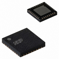
LPC1113FHN33/301,5 NXP Semiconductors, LPC1113FHN33/301,5 Datasheet - Page 43

LPC1113FHN33/301,5
Manufacturer Part Number
LPC1113FHN33/301,5
Description
IC MCU 32BIT 24KB FLASH 33HVQFN
Manufacturer
NXP Semiconductors
Series
LPC1100r
Datasheets
1.LPC1114FHN333015.pdf
(2 pages)
2.LPC1114FHN333015.pdf
(66 pages)
3.LPC1114FHN333015.pdf
(66 pages)
4.LPC1113FHN333015.pdf
(60 pages)
Specifications of LPC1113FHN33/301,5
Program Memory Type
FLASH
Program Memory Size
24KB (24K x 8)
Package / Case
33-VQFN Exposed Pad, 33-HVQFN, 33-SQFN, 33-DHVQFN
Core Processor
ARM Cortex-M0
Core Size
32-Bit
Speed
50MHz
Connectivity
I²C, SPI, UART/USART
Peripherals
Brown-out Detect/Reset, POR, WDT
Number Of I /o
28
Ram Size
8K x 8
Voltage - Supply (vcc/vdd)
1.8 V ~ 3.6 V
Data Converters
A/D 8x10b
Oscillator Type
Internal
Operating Temperature
-40°C ~ 85°C
Processor Series
LPC11
Core
ARM Cortex M0
Data Bus Width
32 bit
Data Ram Size
8 KB
Interface Type
I2C, SPI, UART
Number Of Programmable I/os
28
Operating Supply Voltage
1.8 V to 3.6 V
Maximum Operating Temperature
+ 85 C
Mounting Style
SMD/SMT
3rd Party Development Tools
MDK-ARM, RL-ARM, ULINK2
Minimum Operating Temperature
- 40 C
On-chip Adc
10 bit, 8 Channel
Cpu Family
LPC1100
Device Core
ARM Cortex M0
Device Core Size
32b
Frequency (max)
50MHz
Total Internal Ram Size
8KB
# I/os (max)
42
Number Of Timers - General Purpose
4
Operating Supply Voltage (typ)
3.3V
Operating Supply Voltage (max)
3.6V
Operating Supply Voltage (min)
1.8V
Instruction Set Architecture
RISC
Operating Temp Range
-40C to 85C
Operating Temperature Classification
Industrial
Mounting
Surface Mount
Pin Count
33
Package Type
HVQFN EP
Package
33HVQFN EP
Family Name
LPC1100
Maximum Speed
50 MHz
Number Of Timers
4
Lead Free Status / RoHS Status
Lead free / RoHS Compliant
For Use With
622-1005 - USB IN-CIRCUIT PROG ARM7 LPC2K
Eeprom Size
-
Lead Free Status / Rohs Status
Lead free / RoHS Compliant
Other names
568-4951
935290776551
935290776551
NXP Semiconductors
10. Dynamic characteristics
LPC1111_12_13_14
Product data sheet
10.1 Flash memory
10.2 External clock
Table 11.
T
[1]
[2]
Table 12.
T
[1]
[2]
Symbol
N
t
t
t
Symbol
f
T
t
t
t
t
ret
er
prog
osc
CHCX
CLCX
CLCH
CHCL
amb
amb
Fig 19. External clock timing (with an amplitude of at least V
cy(clk)
endu
Number of program/erase cycles.
Programming times are given for writing 256 bytes from RAM to the flash. Data must be written to the flash
in blocks of 256 bytes.
Parameters are valid over operating temperature range unless otherwise specified.
Typical ratings are not guaranteed. The values listed are at room temperature (25 °C), nominal supply
voltages.
= −40 °C to +85 °C, unless otherwise specified.
= −40 °C to +85 °C; V
Flash characteristics
Dynamic characteristic: external clock
Parameter
oscillator frequency
clock cycle time
clock HIGH time
clock LOW time
clock rise time
clock fall time
Parameter
endurance
retention time
erase time
programming
time
All information provided in this document is subject to legal disclaimers.
Rev. 2 — 18 August 2010
DD
over specified ranges.
Conditions
powered
unpowered
sector or multiple
consecutive
sectors
t
CHCL
Conditions
t
CLCX
[1]
32-bit ARM Cortex-M0 microcontroller
Min
1
40
T
T
-
-
cy(clk)
cy(clk)
[1]
[2]
T
cy(clk)
LPC1111/12/13/14
Min
10000
10
20
95
0.95
× 0.4
× 0.4
t
CLCH
t
CHCX
i(RMS)
Typ
-
-
-
100
1
Typ
-
-
-
-
-
-
= 200 mV)
[2]
002aaa907
© NXP B.V. 2010. All rights reserved.
Max
25
1000
-
-
5
5
Max
-
-
-
105
1.05
Unit
MHz
ns
ns
ns
ns
ns
43 of 60
Unit
cycles
years
years
ms
ms


