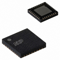
LPC1113FHN33/301,5 NXP Semiconductors, LPC1113FHN33/301,5 Datasheet - Page 26

LPC1113FHN33/301,5
Manufacturer Part Number
LPC1113FHN33/301,5
Description
IC MCU 32BIT 24KB FLASH 33HVQFN
Manufacturer
NXP Semiconductors
Series
LPC1100r
Datasheets
1.LPC1114FHN333015.pdf
(2 pages)
2.LPC1114FHN333015.pdf
(66 pages)
3.LPC1114FHN333015.pdf
(66 pages)
4.LPC1113FHN333015.pdf
(60 pages)
Specifications of LPC1113FHN33/301,5
Program Memory Type
FLASH
Program Memory Size
24KB (24K x 8)
Package / Case
33-VQFN Exposed Pad, 33-HVQFN, 33-SQFN, 33-DHVQFN
Core Processor
ARM Cortex-M0
Core Size
32-Bit
Speed
50MHz
Connectivity
I²C, SPI, UART/USART
Peripherals
Brown-out Detect/Reset, POR, WDT
Number Of I /o
28
Ram Size
8K x 8
Voltage - Supply (vcc/vdd)
1.8 V ~ 3.6 V
Data Converters
A/D 8x10b
Oscillator Type
Internal
Operating Temperature
-40°C ~ 85°C
Processor Series
LPC11
Core
ARM Cortex M0
Data Bus Width
32 bit
Data Ram Size
8 KB
Interface Type
I2C, SPI, UART
Number Of Programmable I/os
28
Operating Supply Voltage
1.8 V to 3.6 V
Maximum Operating Temperature
+ 85 C
Mounting Style
SMD/SMT
3rd Party Development Tools
MDK-ARM, RL-ARM, ULINK2
Minimum Operating Temperature
- 40 C
On-chip Adc
10 bit, 8 Channel
Cpu Family
LPC1100
Device Core
ARM Cortex M0
Device Core Size
32b
Frequency (max)
50MHz
Total Internal Ram Size
8KB
# I/os (max)
42
Number Of Timers - General Purpose
4
Operating Supply Voltage (typ)
3.3V
Operating Supply Voltage (max)
3.6V
Operating Supply Voltage (min)
1.8V
Instruction Set Architecture
RISC
Operating Temp Range
-40C to 85C
Operating Temperature Classification
Industrial
Mounting
Surface Mount
Pin Count
33
Package Type
HVQFN EP
Package
33HVQFN EP
Family Name
LPC1100
Maximum Speed
50 MHz
Number Of Timers
4
Lead Free Status / RoHS Status
Lead free / RoHS Compliant
For Use With
622-1005 - USB IN-CIRCUIT PROG ARM7 LPC2K
Eeprom Size
-
Lead Free Status / Rohs Status
Lead free / RoHS Compliant
Other names
568-4951
935290776551
935290776551
NXP Semiconductors
LPC1111_12_13_14
Product data sheet
7.15.5.1 Sleep mode
7.15.5.2 Deep-sleep mode
7.15.5.3 Deep power-down mode
7.16.1 Start logic
7.16.2 Reset
7.16 System control
When Sleep mode is entered, the clock to the core is stopped. Resumption from the Sleep
mode does not need any special sequence but re-enabling the clock to the ARM core.
In Sleep mode, execution of instructions is suspended until either a reset or interrupt
occurs. Peripheral functions continue operation during Sleep mode and may generate
interrupts to cause the processor to resume execution. Sleep mode eliminates dynamic
power used by the processor itself, memory systems and related controllers, and internal
buses.
In Deep-sleep mode, the chip is in Sleep mode, and in addition all analog blocks are shut
down. As an exception, the user has the option to keep the watchdog oscillator and the
BOD circuit running for self-timed wake-up and BOD protection. Deep-sleep mode allows
for additional power savings.
Up to 13 pins total serve as external wake-up pins to the start logic to wake up the chip
from Deep-sleep mode.
Unless the watchdog oscillator is selected to run in Deep-sleep mode, the clock source
should be switched to IRC before entering Deep-sleep mode, because the IRC can be
switched on and off glitch-free.
In Deep power-down mode, power is shut off to the entire chip with the exception of the
WAKEUP pin. The LPC1111/12/13/14 can wake up from Deep power-down mode via the
WAKEUP pin.
The start logic connects external pins to corresponding interrupts in the NVIC. Each pin
shown in
NVIC interrupt vector table. The start logic pins can serve as external interrupt pins when
the chip is running. In addition, an input signal on the start logic pins can wake up the chip
from Deep-sleep mode when all clocks are shut down.
The start logic must be configured in the system configuration block and in the NVIC
before being used.
Reset has four sources on the LPC1111/12/13/14: the RESET pin, the Watchdog reset,
power-on reset (POR), and the BrownOut Detection (BOD) circuit. The RESET pin is a
Schmitt trigger input pin. Assertion of chip reset by any source, once the operating voltage
attains a usable level, starts the IRC and initializes the flash controller.
When the internal Reset is removed, the processor begins executing at address 0, which
is initially the Reset vector mapped from the boot block. At that point, all of the processor
and peripheral registers have been initialized to predetermined values.
Table 3
All information provided in this document is subject to legal disclaimers.
to
Table 5
Rev. 2 — 18 August 2010
as input to the start logic has an individual interrupt in the
32-bit ARM Cortex-M0 microcontroller
LPC1111/12/13/14
© NXP B.V. 2010. All rights reserved.
26 of 60


