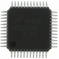
MC908AP32CFAE Freescale Semiconductor, MC908AP32CFAE Datasheet - Page 42

MC908AP32CFAE
Manufacturer Part Number
MC908AP32CFAE
Description
IC MCU 32K FLASH 8MHZ 48-LQFP
Manufacturer
Freescale Semiconductor
Series
HC08r
Specifications of MC908AP32CFAE
Core Processor
HC08
Core Size
8-Bit
Speed
8MHz
Connectivity
I²C, IRSCI, SCI, SPI
Peripherals
LED, LVD, POR, PWM
Number Of I /o
32
Program Memory Size
32KB (32K x 8)
Program Memory Type
FLASH
Ram Size
2K x 8
Voltage - Supply (vcc/vdd)
2.7 V ~ 5.5 V
Data Converters
A/D 8x10b
Oscillator Type
Internal
Operating Temperature
-40°C ~ 85°C
Package / Case
48-LQFP
Controller Family/series
HC08
No. Of I/o's
32
Ram Memory Size
2KB
Cpu Speed
8MHz
No. Of Timers
2
Embedded Interface Type
I2C, SCI, SPI
Rohs Compliant
Yes
Lead Free Status / RoHS Status
Lead free / RoHS Compliant
Eeprom Size
-
Available stocks
Company
Part Number
Manufacturer
Quantity
Price
Company:
Part Number:
MC908AP32CFAE
Manufacturer:
Freescale Semiconductor
Quantity:
10 000
Company:
Part Number:
MC908AP32CFAER
Manufacturer:
Freescale Semiconductor
Quantity:
10 000
- Current page: 42 of 316
- Download datasheet (2Mb)
Memory
Before processing an interrupt, the CPU uses five bytes of the stack to save the contents of the CPU
registers.
During a subroutine call, the CPU uses two bytes of the stack to store the return address. The stack
pointer decrements during pushes and increments during pulls.
2.5 FLASH Memory
This sub-section describes the operation of the embedded FLASH memory. This memory can be read,
programmed, and erased from a single external supply. The program and erase operations are enabled
through the use of an internal charge pump.
2.5.1 Functional Description
The FLASH memory consists of an array of 62,368 bytes for user memory plus a block of 48 bytes for
user interrupt vectors and one byte for the mask option register. An erased bit reads as logic 1 and a
programmed bit reads as a logic 0. The FLASH memory page size is defined as 512 bytes, and is the
minimum size that can be erased in a page erase operation. Program and erase operations are facilitated
through control bits in FLASH control register (FLCR). The address ranges for the FLASH memory are:
Programming tools are available from Freescale. Contact your local Freescale representative for more
information.
1. No security feature is absolutely secure. However, Freescale’s strategy is to make reading or copying the FLASH difficult for
unauthorized users.
42
•
•
•
$0860–$FBFF; user memory, 62,368 bytes
$FFD0–$FFFF; user interrupt vectors, 48 bytes
$FFCF; mask option register
Be careful when using nested subroutines. The CPU may overwrite data in
the RAM during a subroutine or during the interrupt stacking operation.
MC68HC908AP64A
MC68HC908AP32A
MC68HC908AP16A
MC68HC908AP8A
A security feature prevents viewing of the FLASH contents.
Device
For M6805 compatibility, the H register is not stacked.
MC68HC908AP A-Family Data Sheet, Rev. 3
FLASH Memory Size
NOTE
NOTE
(Bytes)
NOTE
62,368
32,768
16,384
8,192
Memory Address Range
$0860–$FBFF
$0860–$885F
$0860–$485F
$0860–$285F
(1)
Freescale Semiconductor
Related parts for MC908AP32CFAE
Image
Part Number
Description
Manufacturer
Datasheet
Request
R
Part Number:
Description:
Manufacturer:
Freescale Semiconductor, Inc
Datasheet:
Part Number:
Description:
Manufacturer:
Freescale Semiconductor, Inc
Datasheet:
Part Number:
Description:
Manufacturer:
Freescale Semiconductor, Inc
Datasheet:
Part Number:
Description:
Manufacturer:
Freescale Semiconductor, Inc
Datasheet:
Part Number:
Description:
Manufacturer:
Freescale Semiconductor, Inc
Datasheet:
Part Number:
Description:
Manufacturer:
Freescale Semiconductor, Inc
Datasheet:
Part Number:
Description:
Manufacturer:
Freescale Semiconductor, Inc
Datasheet:
Part Number:
Description:
Manufacturer:
Freescale Semiconductor, Inc
Datasheet:
Part Number:
Description:
Manufacturer:
Freescale Semiconductor, Inc
Datasheet:
Part Number:
Description:
Manufacturer:
Freescale Semiconductor, Inc
Datasheet:
Part Number:
Description:
Manufacturer:
Freescale Semiconductor, Inc
Datasheet:
Part Number:
Description:
Manufacturer:
Freescale Semiconductor, Inc
Datasheet:
Part Number:
Description:
Manufacturer:
Freescale Semiconductor, Inc
Datasheet:
Part Number:
Description:
Manufacturer:
Freescale Semiconductor, Inc
Datasheet:
Part Number:
Description:
Manufacturer:
Freescale Semiconductor, Inc
Datasheet:


