MC908AP32CFAE Freescale Semiconductor, MC908AP32CFAE Datasheet - Page 139
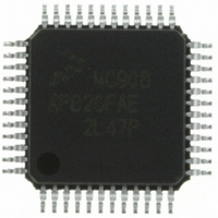
MC908AP32CFAE
Manufacturer Part Number
MC908AP32CFAE
Description
IC MCU 32K FLASH 8MHZ 48-LQFP
Manufacturer
Freescale Semiconductor
Series
HC08r
Specifications of MC908AP32CFAE
Core Processor
HC08
Core Size
8-Bit
Speed
8MHz
Connectivity
I²C, IRSCI, SCI, SPI
Peripherals
LED, LVD, POR, PWM
Number Of I /o
32
Program Memory Size
32KB (32K x 8)
Program Memory Type
FLASH
Ram Size
2K x 8
Voltage - Supply (vcc/vdd)
2.7 V ~ 5.5 V
Data Converters
A/D 8x10b
Oscillator Type
Internal
Operating Temperature
-40°C ~ 85°C
Package / Case
48-LQFP
Controller Family/series
HC08
No. Of I/o's
32
Ram Memory Size
2KB
Cpu Speed
8MHz
No. Of Timers
2
Embedded Interface Type
I2C, SCI, SPI
Rohs Compliant
Yes
Lead Free Status / RoHS Status
Lead free / RoHS Compliant
Eeprom Size
-
Available stocks
Company
Part Number
Manufacturer
Quantity
Price
Company:

Part Number:
MC908AP32CFAE
Manufacturer:
Freescale Semiconductor
Quantity:
10 000
Company:
Part Number:
MC908AP32CFAER
Manufacturer:
Freescale Semiconductor
Quantity:
10 000


To allow software to clear status bits during a break interrupt, write a logic 1 to the BCFE bit. If a status
bit is cleared during the break state, it remains cleared when the MCU exits the break state.
To protect status bits during the break state, write a logic 0 to the BCFE bit. With BCFE at logic 0 (its
default state), software can read and write I/O registers during the break state without affecting status bits.
Some status bits have a 2-step read/write clearing procedure. If software does the first step on such a bit
before the break, the bit cannot change during the break state as long as BCFE is at logic 0. After the
break, doing the second step clears the status bit.
9.8 I/O Signals
Port B shares four of its pins with the TIM. The four TIM channel I/O pins are T1CH0, T1CH1, T2CH0,
and T2CH1 as described in
Each channel I/O pin is programmable independently as an input capture pin or an output compare pin.
T1CH0 and T2CH0 can be configured as buffered output compare or buffered PWM pins.
9.9 I/O Registers
These I/O registers control and monitor operation of the TIM:
9.9.1 TIM Status and Control Register
The TIM status and control register (TSC):
Freescale Semiconductor
•
•
•
•
•
•
•
•
•
•
TIM status and control register (TSC)
TIM counter registers (TCNTH:TCNTL)
TIM counter modulo registers (TMODH:TMODL)
TIM channel status and control registers (TSC0, TSC1)
TIM channel registers (TCH0H:TCH0L, TCH1H:TCH1L)
Enables TIM overflow interrupts
Flags TIM overflows
Stops the TIM counter
Resets the TIM counter
Prescales the TIM counter clock
Address: T1SC, $0020 and T2SC, $002B
References to either timer 1 or timer 2 may be made in the following text by
omitting the timer number. For example, TSC may generically refer to both
T1SC AND T2SC.
Reset:
Read:
Write:
Bit 7
TOF
0
0
Figure 9-4. TIM Status and Control Register (TSC)
9.3 Pin Name
= Unimplemented
TOIE
MC68HC908AP A-Family Data Sheet, Rev. 3
6
0
TSTOP
Conventions.
5
1
NOTE
TRST
4
0
0
3
0
0
PS2
2
0
PS1
1
0
Bit 0
PS0
0
I/O Signals
139
Related parts for MC908AP32CFAE
Image
Part Number
Description
Manufacturer
Datasheet
Request
R

Part Number:
Description:
Manufacturer:
Freescale Semiconductor, Inc
Datasheet:
Part Number:
Description:
Manufacturer:
Freescale Semiconductor, Inc
Datasheet:
Part Number:
Description:
Manufacturer:
Freescale Semiconductor, Inc
Datasheet:
Part Number:
Description:
Manufacturer:
Freescale Semiconductor, Inc
Datasheet:
Part Number:
Description:
Manufacturer:
Freescale Semiconductor, Inc
Datasheet:
Part Number:
Description:
Manufacturer:
Freescale Semiconductor, Inc
Datasheet:
Part Number:
Description:
Manufacturer:
Freescale Semiconductor, Inc
Datasheet:
Part Number:
Description:
Manufacturer:
Freescale Semiconductor, Inc
Datasheet:
Part Number:
Description:
Manufacturer:
Freescale Semiconductor, Inc
Datasheet:
Part Number:
Description:
Manufacturer:
Freescale Semiconductor, Inc
Datasheet:
Part Number:
Description:
Manufacturer:
Freescale Semiconductor, Inc
Datasheet:
Part Number:
Description:
Manufacturer:
Freescale Semiconductor, Inc
Datasheet:
Part Number:
Description:
Manufacturer:
Freescale Semiconductor, Inc
Datasheet:
Part Number:
Description:
Manufacturer:
Freescale Semiconductor, Inc
Datasheet:
Part Number:
Description:
Manufacturer:
Freescale Semiconductor, Inc
Datasheet: