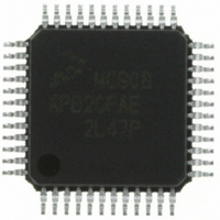
MC908AP32CFAE Freescale Semiconductor, MC908AP32CFAE Datasheet - Page 257

MC908AP32CFAE
Manufacturer Part Number
MC908AP32CFAE
Description
IC MCU 32K FLASH 8MHZ 48-LQFP
Manufacturer
Freescale Semiconductor
Series
HC08r
Specifications of MC908AP32CFAE
Core Processor
HC08
Core Size
8-Bit
Speed
8MHz
Connectivity
I²C, IRSCI, SCI, SPI
Peripherals
LED, LVD, POR, PWM
Number Of I /o
32
Program Memory Size
32KB (32K x 8)
Program Memory Type
FLASH
Ram Size
2K x 8
Voltage - Supply (vcc/vdd)
2.7 V ~ 5.5 V
Data Converters
A/D 8x10b
Oscillator Type
Internal
Operating Temperature
-40°C ~ 85°C
Package / Case
48-LQFP
Controller Family/series
HC08
No. Of I/o's
32
Ram Memory Size
2KB
Cpu Speed
8MHz
No. Of Timers
2
Embedded Interface Type
I2C, SCI, SPI
Rohs Compliant
Yes
Lead Free Status / RoHS Status
Lead free / RoHS Compliant
Eeprom Size
-
Available stocks
Company
Part Number
Manufacturer
Quantity
Price
Company:
Part Number:
MC908AP32CFAE
Manufacturer:
Freescale Semiconductor
Quantity:
10 000
Company:
Part Number:
MC908AP32CFAER
Manufacturer:
Freescale Semiconductor
Quantity:
10 000
- Current page: 257 of 316
- Download datasheet (2Mb)
Chapter 16
Input/Output (I/O) Ports
16.1 Introduction
Thirty-two (32) bidirectional input-output (I/O) pins form four parallel ports. All I/O pins are programmable
as inputs or outputs.
Input pins and I/O port pins that are not used in the application must be terminated. This prevents excess
current caused by floating inputs, and enhances immunity during noise or transient events. Termination
methods include:
Never connect unused pins directly to V
Since some general-purpose I/O pins are not available on all packages, these pins must be terminated
as well. Either method 1 or 2 above are appropriate.
Freescale Semiconductor
$0000
$0001
$0002
$0003
$0004
$0005
$0006
Addr.
1. Configuring unused pins as outputs and driving high or low;
2. Configuring unused pins as inputs and enabling internal pull-ups;
3. Configuring unused pins as inputs and using external pull-up or pull-down resistors.
Port C Data Register (PTC)
Port D Data Register (PTD)
Data Direction Register C
Data Direction Register A
Data Direction Register B
Register Name
Port A Data Register
Port B Data Register
(DDRC)
(DDRA)
(DDRB)
(PTA)
(PTB)
Reset:
Reset:
Reset:
Reset:
Reset:
Reset:
Reset:
Read:
Write:
Read:
Write:
Read:
Write:
Read:
Write:
Read:
Write:
Read:
Write:
Read:
Write:
Figure 16-1. I/O Port Register Summary
MC68HC908AP A-Family Data Sheet, Rev. 3
DDRA7
DDRB7
DDRC7
PTC7
PTD7
PTA7
PTB7
Bit 7
0
0
0
DD
or V
DDRA6
DDRB6
DDRC6
PTC6
PTD6
PTA6
PTB6
6
0
0
0
SS
.
DDRA5
DDRB5
DDRC5
PTC5
PTD5
PTA5
PTB5
5
0
0
0
DDRA4
DDRB4
DDRC4
Unaffected by reset
Unaffected by reset
Unaffected by reset
Unaffected by reset
PTA4
PTB4
PTC4
PTD4
4
0
0
0
DDRC3
DDRA3
DDRB3
PTA3
PTB3
PTC3
PTD3
3
0
0
0
DDRC2
DDRA2
DDRB2
PTA2
PTB2
PTC2
PTD2
2
0
0
0
DDRC1
DDRA1
DDRB1
PTA1
PTB1
PTC1
PTD1
1
0
0
0
DDRA0
DDRB0
DDRC0
PTA0
PTB0
PTC0
PTD0
Bit 0
0
0
0
257
Related parts for MC908AP32CFAE
Image
Part Number
Description
Manufacturer
Datasheet
Request
R
Part Number:
Description:
Manufacturer:
Freescale Semiconductor, Inc
Datasheet:
Part Number:
Description:
Manufacturer:
Freescale Semiconductor, Inc
Datasheet:
Part Number:
Description:
Manufacturer:
Freescale Semiconductor, Inc
Datasheet:
Part Number:
Description:
Manufacturer:
Freescale Semiconductor, Inc
Datasheet:
Part Number:
Description:
Manufacturer:
Freescale Semiconductor, Inc
Datasheet:
Part Number:
Description:
Manufacturer:
Freescale Semiconductor, Inc
Datasheet:
Part Number:
Description:
Manufacturer:
Freescale Semiconductor, Inc
Datasheet:
Part Number:
Description:
Manufacturer:
Freescale Semiconductor, Inc
Datasheet:
Part Number:
Description:
Manufacturer:
Freescale Semiconductor, Inc
Datasheet:
Part Number:
Description:
Manufacturer:
Freescale Semiconductor, Inc
Datasheet:
Part Number:
Description:
Manufacturer:
Freescale Semiconductor, Inc
Datasheet:
Part Number:
Description:
Manufacturer:
Freescale Semiconductor, Inc
Datasheet:
Part Number:
Description:
Manufacturer:
Freescale Semiconductor, Inc
Datasheet:
Part Number:
Description:
Manufacturer:
Freescale Semiconductor, Inc
Datasheet:
Part Number:
Description:
Manufacturer:
Freescale Semiconductor, Inc
Datasheet:


