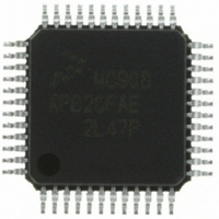
MC908AP32CFAE Freescale Semiconductor, MC908AP32CFAE Datasheet - Page 214

MC908AP32CFAE
Manufacturer Part Number
MC908AP32CFAE
Description
IC MCU 32K FLASH 8MHZ 48-LQFP
Manufacturer
Freescale Semiconductor
Series
HC08r
Specifications of MC908AP32CFAE
Core Processor
HC08
Core Size
8-Bit
Speed
8MHz
Connectivity
I²C, IRSCI, SCI, SPI
Peripherals
LED, LVD, POR, PWM
Number Of I /o
32
Program Memory Size
32KB (32K x 8)
Program Memory Type
FLASH
Ram Size
2K x 8
Voltage - Supply (vcc/vdd)
2.7 V ~ 5.5 V
Data Converters
A/D 8x10b
Oscillator Type
Internal
Operating Temperature
-40°C ~ 85°C
Package / Case
48-LQFP
Controller Family/series
HC08
No. Of I/o's
32
Ram Memory Size
2KB
Cpu Speed
8MHz
No. Of Timers
2
Embedded Interface Type
I2C, SCI, SPI
Rohs Compliant
Yes
Lead Free Status / RoHS Status
Lead free / RoHS Compliant
Eeprom Size
-
Available stocks
Company
Part Number
Manufacturer
Quantity
Price
Company:
Part Number:
MC908AP32CFAE
Manufacturer:
Freescale Semiconductor
Quantity:
10 000
Company:
Part Number:
MC908AP32CFAER
Manufacturer:
Freescale Semiconductor
Quantity:
10 000
- Current page: 214 of 316
- Download datasheet (2Mb)
Serial Peripheral Interface Module (SPI)
The transmit data buffer allows back-to-back transmissions without the slave precisely timing its writes
between transmissions as in a system with a single data buffer. Also, if no new data is written to the data
buffer, the last value contained in the shift register is the next data word to be transmitted.
For an idle master or idle slave that has no data loaded into its transmit buffer, the SPTE is set again no
more than two bus cycles after the transmit buffer empties into the shift register. This allows the user to
queue up a 16-bit value to send. For an already active slave, the load of the shift register cannot occur
until the transmission is completed. This implies that a back-to-back write to the transmit data register is
not possible. The SPTE indicates when the next write can occur.
13.7 Error Conditions
The following flags signal SPI error conditions:
214
•
•
Overflow (OVRF) — Failing to read the SPI data register before the next full byte enters the shift
register sets the OVRF bit. The new byte does not transfer to the receive data register, and the
unread byte still can be read. OVRF is in the SPI status and control register.
Mode fault error (MODF) — The MODF bit indicates that the voltage on the slave select pin (SS)
is inconsistent with the mode of the SPI. MODF is in the SPI status and control register.
CPHA:CPOL = 1:0
WRITE TO SPDR
4 FIRST INCOMING BYTE TRANSFERS FROM SHIFT
5
1
2
3
6 CPU READS SPSCR WITH SPRF BIT SET.
READ SPSCR
CPU WRITES BYTE 1 TO SPDR, CLEARING SPTE BIT.
BYTE 1 TRANSFERS FROM TRANSMIT DATA
REGISTER TO SHIFT REGISTER, SETTING SPTE BIT.
CPU WRITES BYTE 2 TO SPDR, QUEUEING BYTE 2
AND CLEARING SPTE BIT.
REGISTER TO RECEIVE DATA REGISTER, SETTING
SPRF BIT.
BYTE 2 TRANSFERS FROM TRANSMIT DATA
REGISTER TO SHIFT REGISTER, SETTING SPTE BIT.
READ SPDR
SPSCK
SPRF
SPTE
MOSI
1
Figure 13-8. SPRF/SPTE CPU Interrupt Timing
MC68HC908AP A-Family Data Sheet, Rev. 3
MSB BIT
BYTE 1
2
6
BIT
5
3
BIT
4
BIT
3
BIT
2
BIT
1
10
11 CPU READS SPSCR WITH SPRF BIT SET.
12 CPU READS SPDR, CLEARING SPRF BIT.
7 CPU READS SPDR, CLEARING SPRF BIT.
8
9
LSB MSB BIT
5
4
CPU WRITES BYTE 3 TO SPDR, QUEUEING BYTE
SECOND INCOMING BYTE TRANSFERS FROM SHIFT
BYTE 3 TRANSFERS FROM TRANSMIT DATA
3 AND CLEARING SPTE BIT.
REGISTER TO RECEIVE DATA REGISTER, SETTING
SPRF BIT.
REGISTER TO SHIFT REGISTER, SETTING SPTE BIT.
BYTE 2
6
6
7
BIT
5
8
BIT
4
BIT
3
BIT
2
BIT
1
LSB MSB BIT
10
9
BYTE 3
11
6
Freescale Semiconductor
12
BIT
5
BIT
4
Related parts for MC908AP32CFAE
Image
Part Number
Description
Manufacturer
Datasheet
Request
R
Part Number:
Description:
Manufacturer:
Freescale Semiconductor, Inc
Datasheet:
Part Number:
Description:
Manufacturer:
Freescale Semiconductor, Inc
Datasheet:
Part Number:
Description:
Manufacturer:
Freescale Semiconductor, Inc
Datasheet:
Part Number:
Description:
Manufacturer:
Freescale Semiconductor, Inc
Datasheet:
Part Number:
Description:
Manufacturer:
Freescale Semiconductor, Inc
Datasheet:
Part Number:
Description:
Manufacturer:
Freescale Semiconductor, Inc
Datasheet:
Part Number:
Description:
Manufacturer:
Freescale Semiconductor, Inc
Datasheet:
Part Number:
Description:
Manufacturer:
Freescale Semiconductor, Inc
Datasheet:
Part Number:
Description:
Manufacturer:
Freescale Semiconductor, Inc
Datasheet:
Part Number:
Description:
Manufacturer:
Freescale Semiconductor, Inc
Datasheet:
Part Number:
Description:
Manufacturer:
Freescale Semiconductor, Inc
Datasheet:
Part Number:
Description:
Manufacturer:
Freescale Semiconductor, Inc
Datasheet:
Part Number:
Description:
Manufacturer:
Freescale Semiconductor, Inc
Datasheet:
Part Number:
Description:
Manufacturer:
Freescale Semiconductor, Inc
Datasheet:
Part Number:
Description:
Manufacturer:
Freescale Semiconductor, Inc
Datasheet:


