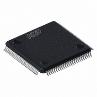
LPC2387FBD100,551 NXP Semiconductors, LPC2387FBD100,551 Datasheet - Page 33

LPC2387FBD100,551
Manufacturer Part Number
LPC2387FBD100,551
Description
IC ARM7 MCU FLASH 512K 100LQFP
Manufacturer
NXP Semiconductors
Series
LPC2300r
Specifications of LPC2387FBD100,551
Program Memory Type
FLASH
Program Memory Size
512KB (512K x 8)
Package / Case
100-LQFP
Core Processor
ARM7
Core Size
16/32-Bit
Speed
72MHz
Connectivity
CAN, Ethernet, I²C, Microwire, MMC, SPI, SSI, SSP, UART/USART, USB OTG
Peripherals
Brown-out Detect/Reset, DMA, I²S, POR, PWM, WDT
Number Of I /o
70
Ram Size
98K x 8
Voltage - Supply (vcc/vdd)
3 V ~ 3.6 V
Data Converters
A/D 6x10b; D/A 1x10b
Oscillator Type
Internal
Operating Temperature
-40°C ~ 85°C
Processor Series
LPC23
Core
ARM7TDMI-S
Data Bus Width
16 bit, 32 bit
Data Ram Size
98 KB
Interface Type
CAN/I2C/I2S/SSP/UART/USB
Maximum Clock Frequency
72 MHz
Number Of Programmable I/os
70
Number Of Timers
4
Operating Supply Voltage
3.3 V
Maximum Operating Temperature
+ 85 C
Mounting Style
SMD/SMT
3rd Party Development Tools
MDK-ARM, RL-ARM, ULINK2, MCB2387, MCB2387U, MCB2387UME
Development Tools By Supplier
OM11013
Minimum Operating Temperature
- 40 C
On-chip Adc
6-ch x 10-bit
On-chip Dac
1-ch x 10-bit
Cpu Family
LPC2000
Device Core
ARM7TDMI-S
Device Core Size
16/32Bit
Frequency (max)
72MHz
Total Internal Ram Size
98KB
# I/os (max)
70
Number Of Timers - General Purpose
4
Operating Supply Voltage (typ)
3.3V
Operating Supply Voltage (max)
3.6V
Operating Supply Voltage (min)
3V
Instruction Set Architecture
RISC
Operating Temp Range
-40C to 85C
Operating Temperature Classification
Industrial
Mounting
Surface Mount
Pin Count
100
Package Type
LQFP
Lead Free Status / RoHS Status
Lead free / RoHS Compliant
For Use With
568-4359 - BOARD EVAL FOR LPC2387568-4310 - EVAL BOARD LPC2158 W/LCD568-3999 - BOARD EVAL FOR LPC23 ARM MCU622-1005 - USB IN-CIRCUIT PROG ARM7 LPC2K
Eeprom Size
-
Lead Free Status / Rohs Status
Compliant
Other names
568-4322
935284932551
LPC2387FBD100-S
935284932551
LPC2387FBD100-S
Available stocks
Company
Part Number
Manufacturer
Quantity
Price
Company:
Part Number:
LPC2387FBD100,551
Manufacturer:
NXP Semiconductors
Quantity:
10 000
NXP Semiconductors
LPC2387
Product data sheet
7.25.5 External interrupt inputs
7.25.6 Memory mapping control
7.26.1 EmbeddedICE
7.26.2 Embedded trace
7.26 Emulation and debugging
The second AHB, referred to as AHB2, includes only the Ethernet block and an
associated 16 kB SRAM. In addition, a bus bridge is provided that allows the secondary
AHB to be a bus master on AHB1, allowing expansion of Ethernet buffer space into
unused space in memory residing on AHB1.
In summary, bus masters with access to AHB1 are the ARM7 itself, the USB block, the
GPDMA function, and the Ethernet block (via the bus bridge from AHB2). Bus masters
with access to AHB2 are the ARM7 and the Ethernet block.
The LPC2387 include up to 46 edge sensitive interrupt inputs combined with up to four
level sensitive external interrupt inputs as selectable pin functions. The external interrupt
inputs can optionally be used to wake up the processor from Power-down mode.
The memory mapping control alters the mapping of the interrupt vectors that appear at the
beginning at address 0x0000 0000. Vectors may be mapped to the bottom of the Boot
ROM or the SRAM. This allows code running in different memory spaces to have control
of the interrupts.
The LPC2387 supports emulation and debugging via a JTAG serial port. A trace port
allows tracing program execution. Debugging and trace functions are multiplexed only
with GPIOs on P2[0] to P2[9]. This means that all communication, timer, and interface
peripherals residing on other pins are available during the development and debugging
phase as they are when the application is run in the embedded system itself.
The EmbeddedICE logic provides on-chip debug support. The debugging of the target
system requires a host computer running the debugger software and an EmbeddedICE
protocol convertor. The EmbeddedICE protocol convertor converts the Remote Debug
Protocol commands to the JTAG data needed to access the ARM7TDMI-S core present
on the target system.
The ARM core has a Debug Communication Channel (DCC) function built-in. The DCC
allows a program running on the target to communicate with the host debugger or another
separate host without stopping the program flow or even entering the debug state. The
DCC is accessed as a co-processor 14 by the program running on the ARM7TDMI-S
core. The DCC allows the JTAG port to be used for sending and receiving data without
affecting the normal program flow. The DCC data and control registers are mapped in to
addresses in the EmbeddedICE logic.
The JTAG clock (TCK) must be slower than
interface to operate.
Since the LPC2387 has significant amounts of on-chip memories, it is not possible to
determine how the processor core is operating simply by observing the external pins. The
ETM provides real-time trace capability for deeply embedded processor cores. It outputs
All information provided in this document is subject to legal disclaimers.
Rev. 4 — 10 February 2011
1
⁄
6
of the CPU clock (CCLK) for the JTAG
Single-chip 16-bit/32-bit MCU
LPC2387
© NXP B.V. 2011. All rights reserved.
33 of 64


