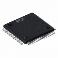
LPC2387FBD100,551 NXP Semiconductors, LPC2387FBD100,551 Datasheet - Page 31

LPC2387FBD100,551
Manufacturer Part Number
LPC2387FBD100,551
Description
IC ARM7 MCU FLASH 512K 100LQFP
Manufacturer
NXP Semiconductors
Series
LPC2300r
Specifications of LPC2387FBD100,551
Program Memory Type
FLASH
Program Memory Size
512KB (512K x 8)
Package / Case
100-LQFP
Core Processor
ARM7
Core Size
16/32-Bit
Speed
72MHz
Connectivity
CAN, Ethernet, I²C, Microwire, MMC, SPI, SSI, SSP, UART/USART, USB OTG
Peripherals
Brown-out Detect/Reset, DMA, I²S, POR, PWM, WDT
Number Of I /o
70
Ram Size
98K x 8
Voltage - Supply (vcc/vdd)
3 V ~ 3.6 V
Data Converters
A/D 6x10b; D/A 1x10b
Oscillator Type
Internal
Operating Temperature
-40°C ~ 85°C
Processor Series
LPC23
Core
ARM7TDMI-S
Data Bus Width
16 bit, 32 bit
Data Ram Size
98 KB
Interface Type
CAN/I2C/I2S/SSP/UART/USB
Maximum Clock Frequency
72 MHz
Number Of Programmable I/os
70
Number Of Timers
4
Operating Supply Voltage
3.3 V
Maximum Operating Temperature
+ 85 C
Mounting Style
SMD/SMT
3rd Party Development Tools
MDK-ARM, RL-ARM, ULINK2, MCB2387, MCB2387U, MCB2387UME
Development Tools By Supplier
OM11013
Minimum Operating Temperature
- 40 C
On-chip Adc
6-ch x 10-bit
On-chip Dac
1-ch x 10-bit
Cpu Family
LPC2000
Device Core
ARM7TDMI-S
Device Core Size
16/32Bit
Frequency (max)
72MHz
Total Internal Ram Size
98KB
# I/os (max)
70
Number Of Timers - General Purpose
4
Operating Supply Voltage (typ)
3.3V
Operating Supply Voltage (max)
3.6V
Operating Supply Voltage (min)
3V
Instruction Set Architecture
RISC
Operating Temp Range
-40C to 85C
Operating Temperature Classification
Industrial
Mounting
Surface Mount
Pin Count
100
Package Type
LQFP
Lead Free Status / RoHS Status
Lead free / RoHS Compliant
For Use With
568-4359 - BOARD EVAL FOR LPC2387568-4310 - EVAL BOARD LPC2158 W/LCD568-3999 - BOARD EVAL FOR LPC23 ARM MCU622-1005 - USB IN-CIRCUIT PROG ARM7 LPC2K
Eeprom Size
-
Lead Free Status / Rohs Status
Compliant
Other names
568-4322
935284932551
LPC2387FBD100-S
935284932551
LPC2387FBD100-S
Available stocks
Company
Part Number
Manufacturer
Quantity
Price
Company:
Part Number:
LPC2387FBD100,551
Manufacturer:
NXP Semiconductors
Quantity:
10 000
NXP Semiconductors
LPC2387
Product data sheet
7.24.4.5 Power domains
7.25.1 Reset
7.25 System control
If power is supplied to the LPC2387 during Deep power-down mode, wake-up can be
caused by the RTC Alarm interrupt or by external Reset.
While in Deep power-down mode, external device power may be removed. In this case,
the LPC2387 will start up when external power is restored.
Essential data may be retained through Deep power-down mode (or through complete
powering off of the chip) by storing data in the Battery RAM, as long as the external power
to the VBAT pin is maintained.
The LPC2387 provides two independent power domains that allow the bulk of the device
to have power removed while maintaining operation of the RTC and the battery RAM.
On the LPC2387, I/O pads are powered by the 3.3 V (V
V
the CPU and most of the peripherals.
Depending on the LPC2387 application, a design can use two power options to manage
power consumption.
The first option assumes that power consumption is not a concern and the design ties the
V
supply for both pads, the CPU, and peripherals. While this solution is simple, it does not
support powering down the I/O pad ring “on the fly” while keeping the CPU and
peripherals alive.
The second option uses two power supplies; a 3.3 V supply for the I/O pads (V
a dedicated 3.3 V supply for the CPU (V
converter powered independently from the I/O pad ring enables shutting down of the I/O
pad power supply “on the fly”, while the CPU and peripherals stay active.
The VBAT pin supplies power only to the RTC and the battery RAM. These two functions
require a minimum of power to operate, which can be supplied by an external battery.
When the CPU and the rest of chip functions are stopped and power removed, the RTC
can supply an alarm output that may be used by external hardware to restore chip power
and resume operation.
Reset has four sources on the LPC2387: the RESET pin, the Watchdog reset, power-on
reset, and the BrownOut Detection (BOD) circuit. The RESET pin is a Schmitt trigger input
pin. Assertion of chip Reset by any source, once the operating voltage attains a usable
level, starts the Wake-up timer (see description in
causing reset to remain asserted until the external Reset is de-asserted, the oscillator is
running, a fixed number of clocks have passed, and the flash controller has completed its
initialization.
When the internal Reset is removed, the processor begins executing at address 0, which
is initially the Reset vector mapped from the Boot Block. At that point, all of the processor
and peripheral registers have been initialized to predetermined values.
DD(DCDC)(3V3)
DD(3V3)
and V
pin powers the on-chip DC-to-DC converter which in turn provides power to
DD(DCDC)(3V3)
All information provided in this document is subject to legal disclaimers.
Rev. 4 — 10 February 2011
pins together. This approach requires only one 3.3 V power
DD(DCDC)(3V3)
Section 7.24.3 “Wake-up
). Having the on-chip DC-to-DC
DD(3V3)
Single-chip 16-bit/32-bit MCU
) pins, while the
LPC2387
© NXP B.V. 2011. All rights reserved.
timer”),
DD(3V3)
31 of 64
) and


