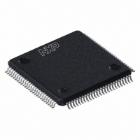
LPC2387FBD100,551 NXP Semiconductors, LPC2387FBD100,551 Datasheet - Page 12

LPC2387FBD100,551
Manufacturer Part Number
LPC2387FBD100,551
Description
IC ARM7 MCU FLASH 512K 100LQFP
Manufacturer
NXP Semiconductors
Series
LPC2300r
Specifications of LPC2387FBD100,551
Program Memory Type
FLASH
Program Memory Size
512KB (512K x 8)
Package / Case
100-LQFP
Core Processor
ARM7
Core Size
16/32-Bit
Speed
72MHz
Connectivity
CAN, Ethernet, I²C, Microwire, MMC, SPI, SSI, SSP, UART/USART, USB OTG
Peripherals
Brown-out Detect/Reset, DMA, I²S, POR, PWM, WDT
Number Of I /o
70
Ram Size
98K x 8
Voltage - Supply (vcc/vdd)
3 V ~ 3.6 V
Data Converters
A/D 6x10b; D/A 1x10b
Oscillator Type
Internal
Operating Temperature
-40°C ~ 85°C
Processor Series
LPC23
Core
ARM7TDMI-S
Data Bus Width
16 bit, 32 bit
Data Ram Size
98 KB
Interface Type
CAN/I2C/I2S/SSP/UART/USB
Maximum Clock Frequency
72 MHz
Number Of Programmable I/os
70
Number Of Timers
4
Operating Supply Voltage
3.3 V
Maximum Operating Temperature
+ 85 C
Mounting Style
SMD/SMT
3rd Party Development Tools
MDK-ARM, RL-ARM, ULINK2, MCB2387, MCB2387U, MCB2387UME
Development Tools By Supplier
OM11013
Minimum Operating Temperature
- 40 C
On-chip Adc
6-ch x 10-bit
On-chip Dac
1-ch x 10-bit
Cpu Family
LPC2000
Device Core
ARM7TDMI-S
Device Core Size
16/32Bit
Frequency (max)
72MHz
Total Internal Ram Size
98KB
# I/os (max)
70
Number Of Timers - General Purpose
4
Operating Supply Voltage (typ)
3.3V
Operating Supply Voltage (max)
3.6V
Operating Supply Voltage (min)
3V
Instruction Set Architecture
RISC
Operating Temp Range
-40C to 85C
Operating Temperature Classification
Industrial
Mounting
Surface Mount
Pin Count
100
Package Type
LQFP
Lead Free Status / RoHS Status
Lead free / RoHS Compliant
For Use With
568-4359 - BOARD EVAL FOR LPC2387568-4310 - EVAL BOARD LPC2158 W/LCD568-3999 - BOARD EVAL FOR LPC23 ARM MCU622-1005 - USB IN-CIRCUIT PROG ARM7 LPC2K
Eeprom Size
-
Lead Free Status / Rohs Status
Compliant
Other names
568-4322
935284932551
LPC2387FBD100-S
935284932551
LPC2387FBD100-S
Available stocks
Company
Part Number
Manufacturer
Quantity
Price
Company:
Part Number:
LPC2387FBD100,551
Manufacturer:
NXP Semiconductors
Quantity:
10 000
NXP Semiconductors
Table 3.
LPC2387
Product data sheet
Symbol
P3[26]/MAT0[1]/
PWM1[3]
P4[0] to P4[31]
P4[28]/MAT2[0]/
TXD3
P4[29]/MAT2[1]/
RXD3
TDO
TDI
TMS
TRST
TCK
RTCK
RSTOUT
RESET
XTAL1
XTAL2
RTCX1
RTCX2
V
V
V
V
SS
SSA
DD(3V3)
DD(DCDC)(3V3)
Pin description
Pin
26
82
85
1
2
3
4
5
100
14
17
22
23
16
18
15, 31,
41, 55,
72, 97,
83
11
28, 54,
71, 96
13, 42,
84
[1]
[1]
[1]
[1]
[1]
[12]
[1]
[1]
[1]
[7]
[8][9]
[8][9]
[8][10]
[8][10]
[11]
[14]
[1]
…continued
[13]
Type
I/O
O
O
I/O
I/O
O
O
I/O
O
I
O
I
I
I
I
I/O
O
I
I
O
I
O
I
I
I
I
All information provided in this document is subject to legal disclaimers.
Description
P3[26] — General purpose digital input/output pin.
MAT0[1] — Match output for Timer 0, channel 1.
PWM1[3] — Pulse Width Modulator 1, output 3.
Port 4: Port 4 is a 32-bit I/O port with individual direction controls for each bit.
The operation of port 4 pins depends upon the pin function selected via the pin
connect block. Pins 0 through 27, 30, and 31 of this port are not available.
P4[28] — General purpose digital input/output pin.
MAT2[0] — Match output for Timer 2, channel 0.
TXD3 — Transmitter output for UART3.
P4[29] — General purpose digital input/output pin.
MAT2[1] — Match output for Timer 2, channel 1.
RXD3 — Receiver input for UART3.
TDO — Test Data Out for JTAG interface.
TDI — Test Data In for JTAG interface.
TMS — Test Mode Select for JTAG interface.
TRST — Test Reset for JTAG interface.
TCK — Test Clock for JTAG interface. This clock must be slower than
CPU clock (CCLK) for the JTAG interface to operate.
RTCK — JTAG interface control signal.
Note: LOW on this pin while RESET is LOW enables ETM pins (P2[9:0]) to
operate as trace port after reset.
RSTOUT — This is a 3.3 V pin. LOW on this pin indicates LPC2387 being in
Reset state.
Note: This pin is available in LPC2387FBD100 devices only (LQFP100
package).
External reset input: A LOW on this pin resets the device, causing I/O ports and
peripherals to take on their default states, and processor execution to begin at
address 0. TTL with hysteresis, 5 V tolerant.
Input to the oscillator circuit and internal clock generator circuits.
Output from the oscillator amplifier.
Input to the RTC oscillator circuit.
Output from the RTC oscillator circuit.
ground: 0 V reference.
analog ground: 0 V reference. This should nominally be the same voltage as
V
3.3 V supply voltage: This is the power supply voltage for the I/O ports.
3.3 V DC-to-DC converter supply voltage: This is the supply voltage for the
on-chip DC-to-DC converter only.
SS
, but should be isolated to minimize noise and error.
Rev. 4 — 10 February 2011
Single-chip 16-bit/32-bit MCU
LPC2387
© NXP B.V. 2011. All rights reserved.
1
⁄
6
of the
12 of 64


