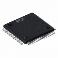
LPC2361FBD100,551 NXP Semiconductors, LPC2361FBD100,551 Datasheet - Page 13

LPC2361FBD100,551
Manufacturer Part Number
LPC2361FBD100,551
Description
IC ARM7 MCU FLASH 64K 100LQFP
Manufacturer
NXP Semiconductors
Series
LPC2300r
Datasheet
1.LPC2361FBD100551.pdf
(57 pages)
Specifications of LPC2361FBD100,551
Program Memory Type
FLASH
Program Memory Size
64KB (64K x 8)
Package / Case
100-LQFP
Core Processor
ARM7
Core Size
16/32-Bit
Speed
72MHz
Connectivity
CAN, I²C, Microwire, SPI, SSI, SSP, UART/USART, USB OTG
Peripherals
Brown-out Detect/Reset, DMA, I²S, POR, PWM, WDT
Number Of I /o
70
Ram Size
34K x 8
Voltage - Supply (vcc/vdd)
3 V ~ 3.6 V
Data Converters
A/D 6x10b; D/A 1x10b
Oscillator Type
Internal
Operating Temperature
-40°C ~ 85°C
Processor Series
LPC23
Core
ARM7TDMI-S
Data Bus Width
16 bit, 32 bit
Data Ram Size
34 KB
Interface Type
CAN/I2S/SPI/SSP/USB
Maximum Clock Frequency
72 MHz
Number Of Programmable I/os
70
Operating Supply Voltage
3.3 V
Maximum Operating Temperature
+ 85 C
Mounting Style
SMD/SMT
3rd Party Development Tools
MDK-ARM, RL-ARM, ULINK2
Minimum Operating Temperature
- 40 C
On-chip Adc
6-ch x 10-bit
On-chip Dac
1-ch x 10-bit
Package
100LQFP
Device Core
ARM7TDMI-S
Family Name
LPC2000
Maximum Speed
72 MHz
Lead Free Status / RoHS Status
Lead free / RoHS Compliant
For Use With
568-4310 - EVAL BOARD LPC2158 W/LCDMCB2360UME - BOARD EVAL MCB2360 + ULINK-MEMCB2360U - BOARD EVAL MCB2360 + ULINK2568-4014 - BOARD EVAL FOR LPC236X ARM568-3999 - BOARD EVAL FOR LPC23 ARM MCU
Eeprom Size
-
Lead Free Status / Rohs Status
Lead free / RoHS Compliant
Other names
568-4525
935286991551
935286991551
Available stocks
Company
Part Number
Manufacturer
Quantity
Price
Company:
Part Number:
LPC2361FBD100,551
Manufacturer:
NXP Semiconductors
Quantity:
10 000
NXP Semiconductors
[3]
[4]
[5]
[6]
[7]
[8]
[9]
[10] Pad provides special analog functionality.
[11] Pad provides special analog functionality.
[12] Pad provides special analog functionality.
[13] Pad provides special analog functionality.
[14] Pad provides special analog functionality.
7. Functional description
LPC2361_62_4
Product data sheet
5 V tolerant pad providing digital I/O with TTL levels and hysteresis and analog output function. When configured as the DAC output,
digital section of the pad is disabled.
Open-drain 5 V tolerant digital I/O pad, compatible with I
output functionality. When power is switched off, this pin connected to the I
Open-drain configuration applies to all functions on this pin.
Pad provides digital I/O and USB functions. It is designed in accordance with the USB specification, revision 2.0 (Full-speed and
Low-speed mode only).
5 V tolerant pad with 5 ns glitch filter providing digital I/O functions with TTL levels and hysteresis.
5 V tolerant pad with 20 ns glitch filter providing digital I/O function with TTL levels and hysteresis.
Pad provides special analog functionality.
When the main oscillator is not used, connect XTAL1 and XTAL2 as follows: XTAL1 can be left floating or can be grounded (grounding
is preferred to reduce susceptibility to noise). XTAL2 should be left floating.
7.1 Architectural overview
The LPC2361/2362 microcontroller consists of an ARM7TDMI-S CPU with emulation
support, the ARM7 local bus for closely coupled, high-speed access to the majority of
on-chip memory, the AMBA AHB interfacing to high-speed on-chip peripherals, and the
AMBA APB for connection to other on-chip peripheral functions. The microcontroller
permanently configures the ARM7TDMI-S processor for little-endian byte order.
The LPC2362 implements two AHBs in order to allow the Ethernet block to operate
without interference caused by other system activity. The primary AHB, referred to as
AHB1, includes the VIC and GPDMA controller.
The second AHB, referred to as AHB2, includes only the Ethernet block and an
associated 16 kB SRAM. In addition, a bus bridge is provided that allows the secondary
AHB to be a bus master on AHB1, allowing expansion of Ethernet buffer space into
off-chip memory or unused space in memory residing on AHB1.
In summary, bus masters with access to AHB1 are the ARM7 itself, the GPDMA function,
and the Ethernet block (via the bus bridge from AHB2). Bus masters with access to AHB2
are the ARM7 and the Ethernet block.
AHB peripherals are allocated a 2 MB range of addresses at the very top of the 4 GB
ARM memory space. Each AHB peripheral is allocated a 16 kB address space within the
AHB address space. Lower speed peripheral functions are connected to the APB. The
AHB to APB bridge interfaces the APB to the AHB. APB peripherals are also allocated a
2 MB range of addresses, beginning at the 3.5 GB address point. Each APB peripheral is
allocated a 16 kB address space within the APB address space.
The ARM7TDMI-S processor is a general purpose 32-bit microprocessor, which offers
high performance and very low power consumption. The ARM architecture is based on
Reduced Instruction Set Computer (RISC) principles, and the instruction set and related
Rev. 04 — 4 March 2010
2
C-bus 400 kHz specification. This pad requires an external pull-up to provide
2
C-bus is floating and does not disturb the I
Single-chip 16-bit/32-bit MCU
LPC2361/62
© NXP B.V. 2010. All rights reserved.
2
C lines.
13 of 57


