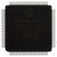
PIC24FJ128GA010-I/PT Microchip Technology, PIC24FJ128GA010-I/PT Datasheet - Page 49

PIC24FJ128GA010-I/PT
Manufacturer Part Number
PIC24FJ128GA010-I/PT
Description
IC PIC MCU FLASH 128K 100TQFP
Manufacturer
Microchip Technology
Series
PIC® 24Fr
Datasheets
1.PIC24FJ16GA002-ISS.pdf
(52 pages)
2.PIC24FJ64GA006-IPT.pdf
(240 pages)
3.PIC24FJ64GA006-IPT.pdf
(22 pages)
4.PIC24FJ128GA008-IPT.pdf
(12 pages)
5.PIC24FJ128GA006-IPT.pdf
(231 pages)
6.PIC24FJ128GA010-IPT.pdf
(230 pages)
Specifications of PIC24FJ128GA010-I/PT
Core Size
16-Bit
Program Memory Size
128KB (43K x 24)
Core Processor
PIC
Speed
16MHz
Connectivity
I²C, PMP, SPI, UART/USART
Peripherals
Brown-out Detect/Reset, POR, PWM, WDT
Number Of I /o
84
Program Memory Type
FLASH
Ram Size
8K x 8
Voltage - Supply (vcc/vdd)
2 V ~ 3.6 V
Data Converters
A/D 16x10b
Oscillator Type
Internal
Operating Temperature
-40°C ~ 85°C
Package / Case
100-TFQFP
Controller Family/series
PIC24
No. Of I/o's
84
Ram Memory Size
8KB
Cpu Speed
32MHz
No. Of Timers
5
No. Of Pwm Channels
5
Embedded Interface Type
EUART, I2C, PSP, SPI
Rohs Compliant
Yes
Processor Series
PIC24FJ
Core
PIC
Data Bus Width
16 bit
Data Ram Size
8 KB
Interface Type
SPI, I2C, USART
Maximum Clock Frequency
16 MHz
Number Of Programmable I/os
54
Number Of Timers
5
Maximum Operating Temperature
+ 85 C
Mounting Style
SMD/SMT
3rd Party Development Tools
52713-733, 52714-737, 53276-922, EWDSPIC
Development Tools By Supplier
PG164130, DV164035, DV244005, DV164005, PG164120, DM240001, DM240011
Minimum Operating Temperature
- 40 C
On-chip Adc
10 bit, 16 Channel
Package
100TQFP
Device Core
PIC
Family Name
PIC24
Maximum Speed
16 MHz
Operating Supply Voltage
2.5|3.3 V
Lead Free Status / RoHS Status
Lead free / RoHS Compliant
For Use With
DM240011 - KIT STARTER MPLAB FOR PIC24F MCUAC164333 - MODULE SKT FOR PM3 100QFPDV164033 - KIT START EXPLORER 16 MPLAB ICD2MA160011 - DAUGHTER BOARD PICDEM LCD 16F91XDM240001 - BOARD DEMO PIC24/DSPIC33/PIC32
Eeprom Size
-
Lead Free Status / Rohs Status
Details
Available stocks
Company
Part Number
Manufacturer
Quantity
Price
Company:
Part Number:
PIC24FJ128GA010-I/PT
Manufacturer:
Microchi
Quantity:
627
Company:
Part Number:
PIC24FJ128GA010-I/PT
Manufacturer:
MICROCHIP
Quantity:
212
Company:
Part Number:
PIC24FJ128GA010-I/PT
Manufacturer:
Microchip Technology
Quantity:
10 000
REGISTER 4-1:
© 2005 Microchip Technology Inc.
Upper Byte:
bit 15
bit 15
bit 14
bit 13
bit 12-7
bit 6
bit 5-4
bit 3-0
R/SO-0
WR
(1)
Legend:
R = Readable bit
-n = Value at Reset
WR: Write Control bit
1 = Initiates a Flash memory program or erase operation
0 = Program or erase operation is complete and inactive
WREN: Write Enable bit
1 = Enable Flash program/erase operations
0 = Inhibit Flash program/erase operations
WRERR: Write Sequence Error Flag bit
1 = An improper program or erase sequence attempt or termination has occurred (bit is set automatically
0 = The program or erase operation completed normally
Unimplemented: Read as ‘0’
ERASE: Erase/Program Enable bit
1 = Perform the erase operation specified by NVMOP3:NVMOP0 on the next WR command
0 = Perform the program operation specified by NVMOP3:NVMOP0 on the next WR command
Unimplemented: Read as ‘0’
NVMOP3:NVMOP0: NVM Operation Select bits
1111 = Memory bulk erase operation (ERASE = 1) or no operation (ERASE = 0)
0010 = Memory row erase operation (ERASE = 1) or no operation (ERASE = 0)
0001 = Memory row program operation (ERASE = 0) or no operation (ERASE = 1)
Note 1: These bits can only be reset on POR.
R/W-0
WREN
The operation is self-timed and the bit is cleared by hardware once operation is complete.
on any set attempt of the WR bit)
Lower Byte:
bit 7
2: All other combinations of NVMOP3:NVMOP0 are unimplemented.
(1)
U-0
—
NVMCOM: FLASH MEMORY CONTROL REGISTER
R/W-0
WRERR
R/W-0
ERASE
(1)
(1)
W = Writable bit
‘1’ = Bit is set
U-0
—
Advance Information
U-0
—
U-0
—
PIC24FJ128GA FAMILY
U-0
—
(2)
SO = Settable-Only bit
‘0’ = Bit is cleared
NVMOP3
R/W-0
U-0
—
(1)
(2)
NVMOP2
U-0
—
R/W-0
(1)
(2)
U-0
U = Unimplemented bit
x = Bit is unknown
NVMOP1
—
R/W-0
bit 8
(1)
DS39747A-page 47
(2)
NVMOP0
R/W-0
bit 0
(1)
(2)


