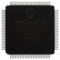
PIC24FJ128GA010-I/PT Microchip Technology, PIC24FJ128GA010-I/PT Datasheet - Page 187

PIC24FJ128GA010-I/PT
Manufacturer Part Number
PIC24FJ128GA010-I/PT
Description
IC PIC MCU FLASH 128K 100TQFP
Manufacturer
Microchip Technology
Series
PIC® 24Fr
Datasheets
1.PIC24FJ16GA002-ISS.pdf
(52 pages)
2.PIC24FJ64GA006-IPT.pdf
(240 pages)
3.PIC24FJ64GA006-IPT.pdf
(22 pages)
4.PIC24FJ128GA008-IPT.pdf
(12 pages)
5.PIC24FJ128GA006-IPT.pdf
(231 pages)
6.PIC24FJ128GA010-IPT.pdf
(230 pages)
Specifications of PIC24FJ128GA010-I/PT
Core Size
16-Bit
Program Memory Size
128KB (43K x 24)
Core Processor
PIC
Speed
16MHz
Connectivity
I²C, PMP, SPI, UART/USART
Peripherals
Brown-out Detect/Reset, POR, PWM, WDT
Number Of I /o
84
Program Memory Type
FLASH
Ram Size
8K x 8
Voltage - Supply (vcc/vdd)
2 V ~ 3.6 V
Data Converters
A/D 16x10b
Oscillator Type
Internal
Operating Temperature
-40°C ~ 85°C
Package / Case
100-TFQFP
Controller Family/series
PIC24
No. Of I/o's
84
Ram Memory Size
8KB
Cpu Speed
32MHz
No. Of Timers
5
No. Of Pwm Channels
5
Embedded Interface Type
EUART, I2C, PSP, SPI
Rohs Compliant
Yes
Processor Series
PIC24FJ
Core
PIC
Data Bus Width
16 bit
Data Ram Size
8 KB
Interface Type
SPI, I2C, USART
Maximum Clock Frequency
16 MHz
Number Of Programmable I/os
54
Number Of Timers
5
Maximum Operating Temperature
+ 85 C
Mounting Style
SMD/SMT
3rd Party Development Tools
52713-733, 52714-737, 53276-922, EWDSPIC
Development Tools By Supplier
PG164130, DV164035, DV244005, DV164005, PG164120, DM240001, DM240011
Minimum Operating Temperature
- 40 C
On-chip Adc
10 bit, 16 Channel
Package
100TQFP
Device Core
PIC
Family Name
PIC24
Maximum Speed
16 MHz
Operating Supply Voltage
2.5|3.3 V
Lead Free Status / RoHS Status
Lead free / RoHS Compliant
For Use With
DM240011 - KIT STARTER MPLAB FOR PIC24F MCUAC164333 - MODULE SKT FOR PM3 100QFPDV164033 - KIT START EXPLORER 16 MPLAB ICD2MA160011 - DAUGHTER BOARD PICDEM LCD 16F91XDM240001 - BOARD DEMO PIC24/DSPIC33/PIC32
Eeprom Size
-
Lead Free Status / Rohs Status
Details
Available stocks
Company
Part Number
Manufacturer
Quantity
Price
Company:
Part Number:
PIC24FJ128GA010-I/PT
Manufacturer:
Microchi
Quantity:
627
Company:
Part Number:
PIC24FJ128GA010-I/PT
Manufacturer:
MICROCHIP
Quantity:
212
Company:
Part Number:
PIC24FJ128GA010-I/PT
Manufacturer:
Microchip Technology
Quantity:
10 000
23.2
All of the PIC24FJ128GA family devices power their
core digital logic at a nominal 2.5V. This may create an
issue for designs that are required to operate at a
higher typical voltage, such as 3.3V. To simplify system
design, all devices in the PIC24FJ128GA family incor-
porate an on-chip regulator that allows the device to
run its core logic from V
The regulator is controlled by the ENVREG pin. Tying
V
vides power to the core from the other V
the regulator is enabled, a low ESR capacitor (such as
tantalum) must be connected to the V
(Figure 23-1). This helps to maintain the stability of the
regulator. The recommended value for the filer capacitor
is provided in Section 26.1 “DC Characteristics”.
If ENVREG is tied to V
this case, separate power for the core logic at a nomi-
nal 2.5V must be supplied to the device on the
V
levels, typically 3.3V. Alternatively, the V
and V
nominal voltage. Refer to Figure 23-1 for possible
configurations.
23.2.1
When the voltage regulator is enabled, it takes approxi-
mately 20 s for it to generate output. During this time,
designated as T
T
operation after any power-down, including Sleep mode.
If the regulator is disabled, a separate Power-up Timer
(PWRT) is automatically enabled. The PWRT adds a
fixed delay of 64 ms nominal delay at device start-up.
23.2.2
When
PIC24FJ128GA family devices also have a simple
brown-out capability. If the voltage supplied to the reg-
ulator is inadequate to maintain a regulated level, the
regulator Reset circuitry will generate a Brown-out
Reset. This event is captured by the BOR flag bit
(RCON<0>). The brown-out voltage levels are specific
in Section 26.1 “DC Characteristics”.
23.2.3
The on-chip regulator is designed to meet the power-up
requirements for the device. If the application does not
use the regulator, then strict power-up conditions must
be adhered to. While powering up, V
never exceed V
© 2005 Microchip Technology Inc.
STARTUP
DD
DDCORE
to the pin enables the regulator, which in turn, pro-
DD
On-Chip Voltage Regulator
pins can be tied together to operate at a lower
/V
the
is applied every time the device resumes
CAP
ON-CHIP REGULATOR AND POR
ON-CHIP REGULATOR AND BOR
POWER-UP REQUIREMENTS
pin to run the I/O pins at higher voltage
DD
STARTUP
on-chip
by 0.3 volts.
SS
DD
, code execution is disabled.
, the regulator is disabled. In
.
regulator
DDCORE
DD
is
DDCORE
DDCORE
pins. When
Advance Information
/V
enabled,
CAP
/V
must
CAP
pin
PIC24FJ128GA FAMILY
FIGURE 23-1:
Note 1:
Regulator Enabled (ENVREG tied to V
Regulator Disabled (ENVREG tied to ground):
Regulator Disabled (V
(10 F typ)
2.5V
C
2.5V
EFC
(1)
These are typical operating voltages. Refer
to Section 26.1 “DC Characteristics” for
the full operating ranges of V
V
(1)
DDCORE
3.3V
3.3V
.
CONNECTIONS FOR THE
ON-CHIP REGULATOR
(1)
V
ENVREG
V
V
DD
DDCORE
SS
DD
PIC24FJ128GA
V
ENVREG
V
V
V
ENVREG
V
V
DD
DDCORE
SS
DD
DDCORE
SS
tied to V
PIC24FJ128GA
PIC24FJ128GA
/V
CAP
DS39747A-page 185
/V
/V
DDCORE
CAP
CAP
DD
and
DD
):
):


